Positive Output Precision Voltage Limiter

Positive Output Precision Voltage Limiter

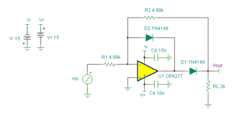
This circuit limits its output to a positive- going output only; negative output is clamped to ground. For negative inputs, D1 conducts and R2 provides negative feedback into U1’s summing junction. For positive inputs, D2 conducts and holds the summing junction to 0V. Thus the output across RL can only be positive. This characteristic is handy when driving single-supply amplifiers or unipolar A/D converters. For a negative output simply reverse D1 & D2. As shown, this circuit is a unity- gain inverter but it is also capable of providing voltage gain. Av = – 2 / R1. (Circuit is created by Neil P. Albaugh,  TI – Tucson)

Positive Output Precision Voltage Limiter circuit:
Positive Output Precision Voltage Limiter


Online Simulation of the Positive Output Precision Voltage Limiter Circuit

The great feature of the TINA circuit simulator that you can analyze this circuit immediately with TINACloud the online version of TINA. Of course you can also run this circuit in the off-line version of TINA.

Click here to invoke TINACloud  and analyze the circuit yourself, or watch our tutorial video! 

You can send this link to any TINACloud customers and they can immediatelly load it by a single click and then run using TINACloud.

Michael Koltai
www.tina.com

Online Simulation of a Transimpedance Amplifier Circuit

Online Simulation of a Transimpedance Amplifier Circuit

This fast photodiode transimpedance amplifier is based on a high- speed JFET- input op amp OPA657.

This op amp is compensated for a minimum closed- loop gain of 7V/V, but the capacitance of the photodiode plus the op amp input capacitance together with the feedback resistor R1 provides a noise gain at high frequency that allows stable operation.

Compensation capacitor C1 optimizes the amplifier bandwidth / gain peaking tradeoff.

Achieving this level of performance requires very careful layout and the circuit must be shielded to prevent noise pickup.

(Circuit is created by Neil P. Albaugh,  TI- Tucson)

Transimpedance amplifier circuit:

transimpedance amplifier-blog

Online Simulation of a Transimpedance Amplifier Circuit

The great feature of the TINA circuit simulator that you can analyze this circuit immediately with TINACloud the online version of TINA. Of course you can also run this circuit in the off-line version of TINA.

Click here to invoke TINACloud and analyze the circuit yourself, or watch our tutorial video!  

You can send this link to any TINACloud customers and they can immediatelly load it by a single click and then run using TINACloud.

Michael Koltai
www.tina.com

Comparator Window Settings

Comparator Window Settings

Conventional window comparators suffer interaction between the width and the center of the window.

This makes adjusting these parameters time consuming.

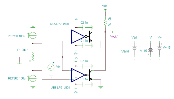
By using a precision dual 100uA current reference (REF200), this interaction is eliminated.

The width of the comparator window is determined by the reference current and the value of P1: V = 100uA * 20k.

The DC voltage of the window center is set by the % rotation of the potentiometer P1.

With the pot at its center (50%), the center of the comparator window is at zero volts– thus the window is +/-1V. The window center adjustment is illustrated below. (Circuit is created by Neil P. Albaugh  TI- Tucson)

Comparator Window Settings circuit:
comparator window settings
Comparator Window Settings
Online Simulation of the Comparator Window Settings Circuit

The great feature of the TINA circuit simulator that you can analyze this circuit immediately with TINACloud the online version of TINA. Of course you can also run this circuit in the off-line version of TINA.

Click here to invoke TINACloud and analyze the circuit yourself, or watch our tutorial video!  

You can send this link to any TINACloud customers and they can immediatelly load it by a single click and then run using TINACloud.

Michael Koltai
www.tina.com
Laser Energy Meter

Laser Energy Meter Circuit

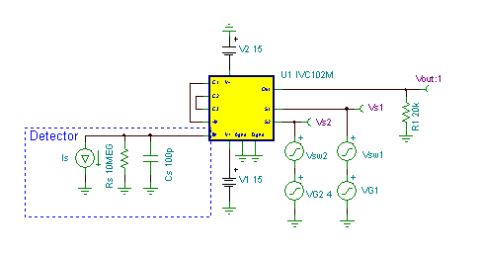
An IVC102 switched integrator is also capable of integrating the output of a very fast detector. By storing the energy of a fast detector current pulse on its own capacitance (or on additional capacitance), this energy can then be transfered to the integrator feedback capacitor where it is held until it is sampled and the integrator can then be reset, awaiting the next pulse. Thus laser energy can be measured on a pulse- by- pulse basis. Needless to say, It is necessary to sync the integrator timing with the laser Q- switch. The simulated detector output pulse was 10mA peak with a 10ns width. Charge is stored on Cs until it is transfered when S1 closes.

To prevent droop error due to shunt resistance Rs and the input bias current of U1,

S1 should be closed a few microseconds after the laser pulse. The IVC102 can integrate a positive- output or negative- output detector. Lower sensitivity can be achieved by paralleling C2, C3, or an external capacitance. Bypass capacitors are not shown.  (Circuit is created by Neil P. Albaugh  TI- Tucson)

 Laser Energy Meter circuit:
Laser Energy meter
Laser Energy Meter
Online Simulation of the Laser Energy Meter Circuit

The great feature of the TINA circuit simulator that you can analyze this circuit immediately with TINACloud the online version of TINA. Of course you can also run this circuit in the off-line version of TINA.

Click here to invoke TINACloud  and analyze the circuit yourself, or watch our tutorial video!

You can send this link to any TINACloud customers and they can immediatelly load it by a single click and then run using TINACloud.

Michael Koltai
www.tina.com
DAC Interface Circuit

DAC Interface Circuit

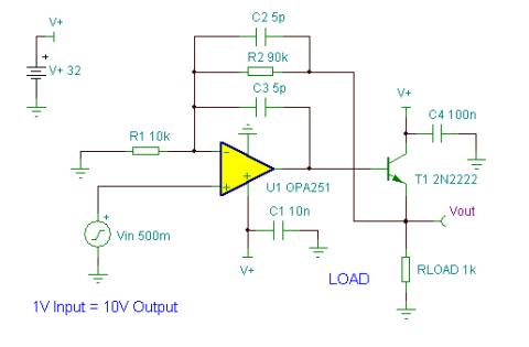
This “DAC Interface”  circuit is a precision buffer amplifier for a DAC output. It is scaled to provide a 10V output @ 10mA with a +1V input voltage. This type of current source can be very useful in industrial interface applications.

A R-R output op amp with an input common-mode range that includes its negative supply rail, such as an OPA251, is required for single- supply operation.

An external NPN transistor  is used to off- load the circuit power dissipation from the precision op amp U1. Re- scaling this circuit with other transistors can result in output current capability of a many amps. (Circuit is created by Neil P. Albaugh  TI – Tucson)

DAC Interface Circuit:
 DAC Interface Circuit
DAC Interface Circuit
Online Simulation of the DAC Interface Circuit

The great feature of the TINA circuit simulator that you can analyze this circuit immediately with TINACloud the online version of TINA. Of course you can also run this circuit in the off-line version of TINA.

Click here to invoke TINACloud  and analyze the circuit yourself, or  watch our tutorial video!

You can send this link to any TINACloud customers and they can immediatelly load it by a single click and then run using TINACloud.

Michael Koltai
www.tina.com