Programming a Terasic Intel FPGA board in VHDL with TINA

Programming a Terasic Intel FPGA board in VHDL with TINA

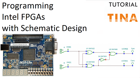
In our previous video, we have shown how you can create a digital circuit and download to an FPGA board by using TINA’s Schematic Editor. (Programming a Terasic Intel FPGA board with TINA using Schematic Design Entry).

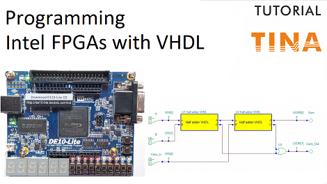
Now, in this video tutorial  our circuit, a full adder, will be based on the VHDL  hardware description language.

As we stated earlier, TINA works with schematics, but we can also place HDL macros, including VHDL and Verilog, in the design.  

Now, let’s see an example, a full adder using the half-adder VHDL macros.

 Start TINA, then open the Full_Adder_VHDL.tsc from the TINA Examples\FPGA folder.

Most digital circuits that perform addition or subtraction use full adder. This combinational circuit adds two binary digits and a carry-in to produce a sum and carry-out. This one-bit full-adder cell has three inputs (A, B, Carry_In) and two outputs (Sum, Carry_Out) by applying a half adder to accept the carry-in (Carry_In) input from the previous less-significant stage of a multiple bit adder. 

The circuit operates like a half adder while the Carry-In value is low. 

Start the simulation by pressing the Dig Interactive button. 

  • When both inputs are low while Carry_In is also low, then Sum and Carry_Out are also low. 
  • When just one input is low while Carry_In is low, then Sum is high and Carry_Out is also low. 
  • When both inputs are high when Carry_In is low, then Sum is low and Carry_Out is high.

Now, let’s see what happens when Carry_In is high.

  • When Carry_In is High while both inputs are low, then Sum is high too and Carry_Out is low. 
  • When Carry_In is High while only one input is high then Sum is low and Carry_Out is also high. 
  • When Carry_In is High while both inputs are high then Sum and Carry_Out are also high. 
If Carry_In is high, then the output values change as if we have added one to the full adder. 

In the following we will test our circuit in a real environment using the  Terasic DE10-Lite FPGA board. 

As it can be seen, this circuit is already prepared for the FPGA Tool export. 

(See our previous video:Programming a Terasic Intel FPGA board with TINA using Schematic Design Entry

In the following we will show how to  generate the source file for Xilinx Vivado 

Finally we will present how our simulated full adder circuit works along with the programmed DE10-Lite hardware.

As you can see, in all cases, the results are exactly the same.

This is a great example of demonstrating the power of simulation, since you can test and debug circuits even before realizing them, and in our case before downloading to FPGA, where if there were any issues, it would be extremely hard to find the problem.

Check our other video “Programming a Terasic Intel FPGA Board in Verilog with TINA”, where we use a Verilog component in FPGA design.

To learn more please click  here.

You can learn more about TINA here: www.tina.com

You can learn more about TINACloud here: www.tinacloud.com

Programming a Terasic Intel FPGA Board with TINACloud using Schematic Design Entry

Programming a Terasic Intel FPGA Board with TINACloud using Schematic Design Entry

In this tutorial video we will show how to create a digital circuit and download it to a Terasic DE10-Lite FPGA board using TINACloud’s Schematic Editor.

In a similar way it is also possible to download digital circuits to the FPGA of DesignSoft’s LabXplorer.

The schematic design may contain gates or other built-in digital components in TINACloud, or macros defining digital components with hardware description languages such as VHDL or Verilog. 

In this video, we will use a free Intel tool, Quartus Prime Lite Edition, which is required for the Intel MAX 10 FPGA, in the Terasic DE10-Lite board.

For other Intel FPGAs, you might need to use the Standard or Pro Edition of Quartus.

These tools will be responsible for creating configuration files for the FPGA programmable logic. 

Now, let’s see an example. 

Start TINACloud, then open the Half_Adder_Gates.tsc file from the TINA Examples folder. 

The half adder is a simple combinational circuit to add two single binary digits and provide the output plus a carry value. It has two inputs called A and B and two outputs called Sum and Carry. 

This schematic diagram contains basic OR, AND, Inverter gates, High-Low switches and Logic Indicators.

To test the circuit, press the Dig interactive button. 

Play with the switches by toggling between low and high levels to produce all the input combinations. 

  • If both inputs are low, then Sum and Carry are also low. 
  • If just one input is high, then Sum is high, and Carry is low. 
  • If both inputs are high, then Sum is low, and Carry is high. 

Now, before testing our circuit in a real FPGA development board environment, we need to extend our schematic with FPGA Pin connectors from the Special toolbar of TINACloud. 

Pin connectors as certain elements such as clocks, push buttons and LEDs are preconnected to the FPGA chips’s pins on the development board. 

The FPGA development tools call them constraints. 

So, we will add 4 FPGA Pin connectors to the circuit’s inputs and outputs, as shown next.

The Device section of the window contains the list of supported boards in the TINACloud system. 

In the Group section, the types of input/output parts (e.g. Switches) of the selected Board (e.g. Digilent Basys) are listed. 

Once you select a type in the Group section (e.g. Switches), in the Pin section the connection pins of the selected type of parts appear (e.g.  SW[0] ). These connection pins should be associated with the corresponding nodes in the TINACloud schematic.  We will rename the FPGA input and output Pins (including their labels) accordingly as those on the FPGA boards (to which they will be connected).

Generating the source file for Intel Quartus Lite

In the following, we will show, how to generate the source file for Intel Quartus Lite.

The qsf – Quartus Prime Settings File – guides the FPGA software on which physical pins on the FPGA will be the inputs and outputs.  The qsf is made from the FPGA pin settings we made previously.  

To produce downloadable content, first we create the Quartus Prime Lite project.  

Testing the simulated Half Adder circuit along with the programmed DE10-Lite hardware. 

At the end of the video we will show how our simulated half adder circuit works along with the  programmed DE10-Lite hardware.

To watch our tutorial and learn more please click  here.

You can learn more about TINA here: www.tina.com

You can learn more about TINACloud here: www.tinacloud.com

Programming a Terasic Intel FPGA board with TINA using Schematic Design Entry

Programming a Terasic Intel FPGA board with TINA using Schematic Design Entry

In this tutorial video, we will show you how to create a digital circuit and download it to a Terasic DE10-Lite FPGA board using  TINA’s Schematic Editor.

In a similar way it is also possible to download digital circuits to the FPGA of DesignSoft’s LabXplorer.

We  will use a free Intel tool, Quartus Prime Lite Edition, which is required for the Intel MAX 10 FPGA in the Terasic DE10-Lite board.

For other Intel FPGAs, you might need to use the Standard or Pro Edition of Quartus.

We presume that the board is accessible from your machine and that the necessary drivers have been installed. 

As demonstration we use a half adder circuit which you can find in the Example folder of TINA.

Before testing our circuit in a real FPGA development board environment, we need to extend our schematic with FPGA Pin connectors. We add 2 Pin connectors to the inputs and 2 Pins to the outputs.

Next, we rename the FPGA input and output Pins (including their labels) accordingly as those on the FPGA boards.

After that, we present how to generate the source file for  Intel Quartus Lite.

TINA always creates a VHD file from any type of representation of the digital circuit.

That is, schematic diagrams, VHDL, Verilog codes or combinations thereof  are always translated  into a VHD file for Quartus.  

The QSF—Quartus Prime Settings— file guides the FPGA software for which the physical pins on the FPGA will be the inputs and outputs. The qsf is made from the FPGA pin settings we made previously.  

To produce downloadable content, we first have to create the Quartus Prime Lite project.  

Testing the simulated Half Adder circuit along with the programmed DE10-Lite hardware. 

As soon as we finish programming the hardware we can start testing our simulated Half Adder circuit and see how it works along with the programmed DE10-Lite hardware.

We will change the virtual switches in TINA by clicking them on the screen, and at the same time we will also change the real switches on the DE10-Lite board. 

  • If both inputs are low, then Sum and Carry are also low. 
  • If just one input is high, then Sum is high and Carry is low.
  • If both inputs are high, then Sum is low and Carry is high.

As you can see, in all cases the results are exactly the same.

This is a great example of demonstrating the power of simulation since you can test and debug circuits even before realizing them, and in our case before downloading to FPGA, where if there were any issues it would be extremely hard to find the problem.

To watch our tutorial and learn more please click  here.

You can learn more about TINA here: www.tina.com

You can learn more about TINACloud here: www.tinacloud.com