In this tutorial video we will show how to create a digital circuit and download it to a Terasic DE10-Lite FPGA board using TINACloud’s Schematic Editor.
In a similar way it is also possible to download digital circuits to the FPGA of DesignSoft’s LabXplorer.
The schematic design may contain gates or other built-in digital components in TINACloud, or macros defining digital components with hardware description languages such as VHDL or Verilog.
In this video, we will use a free Intel tool, Quartus Prime Lite Edition, which is required for the Intel MAX 10 FPGA, in the Terasic DE10-Lite board.
For other Intel FPGAs, you might need to use the Standard or Pro Edition of Quartus.
These tools will be responsible for creating configuration files for the FPGA programmable logic.
Now, let’s see an example.
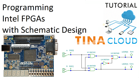
Start TINACloud, then open the Half_Adder_Gates.tsc file from the TINA Examples folder.
The half adder is a simple combinational circuit to add two single binary digits and provide the output plus a carry value. It has two inputs called A and B and two outputs called Sum and Carry.
This schematic diagram contains basic OR, AND, Inverter gates, High-Low switches and Logic Indicators.
To test the circuit, press the Dig interactive button.
Play with the switches by toggling between low and high levels to produce all the input combinations.
- If both inputs are low, then Sum and Carry are also low.
- If just one input is high, then Sum is high, and Carry is low.
- If both inputs are high, then Sum is low, and Carry is high.
Now, before testing our circuit in a real FPGA development board environment, we need to extend our schematic with FPGA Pin connectors from the Special toolbar of TINACloud.
Pin connectors as certain elements such as clocks, push buttons and LEDs are preconnected to the FPGA chips’s pins on the development board.
The FPGA development tools call them constraints.
So, we will add 4 FPGA Pin connectors to the circuit’s inputs and outputs, as shown next.
The Device section of the window contains the list of supported boards in the TINACloud system.
In the Group section, the types of input/output parts (e.g. Switches) of the selected Board (e.g. Digilent Basys) are listed.
Once you select a type in the Group section (e.g. Switches), in the Pin section the connection pins of the selected type of parts appear (e.g. SW[0] ). These connection pins should be associated with the corresponding nodes in the TINACloud schematic. We will rename the FPGA input and output Pins (including their labels) accordingly as those on the FPGA boards (to which they will be connected).
Generating the source file for Intel Quartus Lite
In the following, we will show, how to generate the source file for Intel Quartus Lite.
The qsf – Quartus Prime Settings File – guides the FPGA software on which physical pins on the FPGA will be the inputs and outputs. The qsf is made from the FPGA pin settings we made previously.
To produce downloadable content, first we create the Quartus Prime Lite project.
Testing the simulated Half Adder circuit along with the programmed DE10-Lite hardware.
At the end of the video we will show how our simulated half adder circuit works along with the programmed DE10-Lite hardware.
To watch our tutorial and learn more please click here.
You can learn more about TINA here: www.tina.com
You can learn more about TINACloud here: www.tinacloud.com