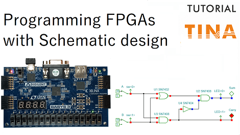
In our other videos, we have shown how you can create a digital circuit and download to an FPGA board by using TINA’s Schematic Editor: (Programming FPGA boards with TINA using Schematic Design Entry)
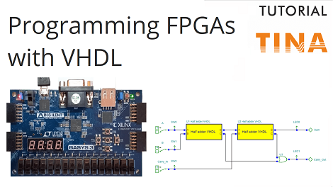
and the VHDL hardware description language: (Programming FPGA boards in VHDL with TINA).
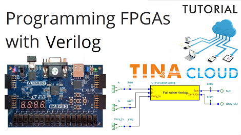
Now, in this video tutorial, our circuit, a full adder, will be based on the Verilog hardware description language.
The textual description of the hardware greatly enhances portability and reusability. By using hardware description languages describing the fundamental operations, structures and connections, virtually any logical circuit can be defined.
As we stated earlier, TINA works with schematics, but we can also place HDL macros, including VHDL and Verilog, in the design.
First we will test our circuit with Verilog circuit simulation in TINA.
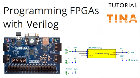
The circuit operates like a half adder while Carry_In value is low.
- When both inputs are low while Carry_In is also low, then Sum and Carry_Out are also low.
- When just one input is low while Carry_In is low, then Sum is high and Carry_Out is also low.
- When both inputs are high when Carry_In is low, then Sum is low and Carry_Out is high.
Now, let’s see what happens when Carry_In is high.
- When Carry_In is high while both inputs are low, then Sum is high too and Carry_Out is low.
- When Carry_In is high while only one input is high, then Sum is low and Carry_Out is also high.
- When Carry_In is high while both inputs are high, then Sum and Carry_Out are also high.
If Carry_in is high, then the output values change as if we had added one to the full adder.
Next we will export the Verilog to the Xilinx Vivado software, compile it and load the resulting bitstream into the Basys 3 FPGA development board.
Finally we will present how our simulated full adder circuit works along with the programmed Basys 3 hardware and show that in all cases, the results are exactly the same.
Check our other video “Programming FPGA Boards in VHDL with TINA”, where we use a Verilog component in FPGA design.
To learn more please click here.
You can learn more about TINA here: www.tina.com
You can learn more about TINACloud here: www.tinacloud.com