In this tutorial video we will show how to create a digital circuit and download it to a Digilent Basys 3 FPGA board by using TINA’s Schematic Editor.
In a similar way it is also possible to download digital circuits to the FPGA of DesignSoft’s LabXplorer.
The schematic design may contain gates or other built-in digital components in TINA. Also it may contain macros defining digital components with hardware description languages such as VHDL or Verilog.
In this video, we use a free Xilinx tool, Vivado, which is required for the FPGA in Digilent Basys 3.
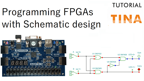
As demonstration we use a half adder circuit which you can find in the Example folder of TINA.
Getting ready to test the circuit in real FPGA development board environment
Before testing our circuit in a real FPGA development board environment, we need to extend our schematic with FPGA Pin connectors. We add 2 Pin connectors to the inputs and 2 Pins to the outputs.
Next, we rename the FPGA input and output Pins (including their labels) accordingly as those on the FPGA boards.
Next, we present how to generate the source file for Xilinx Vivado.
Note that TINA always creates vhd file from any type of
representation of the digital circuit. That is, schematic diagrams, VHDL, Verilog codes or their mix are always translated into a vhd file for Vivado.
The xdc – Xilinx Design Constraints – guides the Xilinx software on which physical pins on the FPGA will be the inputs and outputs. The xdc is made from the FPGA pin settings we made previously.
Creating the Vivado project and programming the hardware
Next, we need to create the Vivado project to produce downloadable content.
As soon as we finish programming the hardware we can start testing our simulated Half Adder circuit and see how it works along with the programmed Basys 3 hardware.
We will change the virtual switches in TINA by clicking them on the screen, and at the same time we will also change the real switches on the Basys 3 board.
- If both inputs are low, then Sum and Carry are also low.
- If just one input is high, then Sum is high and Carry is low.
- If both inputs are high, then Sum is low and Carry is high.
As you can see, in all cases the results are exactly the same.
This is a great example of demonstrating the power of simulation since you can test and debug circuits even before realizing them, and in our case before downloading to FPGA, where if there were any issues it would be extremely hard to find the problem.
To watch our tutorial and learn more please click here.
You can learn more about TINA here: www.tina.com
You can learn more about TINACloud here: www.tinacloud.com