Simulating and downloading Counters to Intel FPGA boards with TINACloud using TINACloud’s Schematic Editor

Simulating and downloading Counters to Intel FPGA boards with TINACloud using TINACloud’s Schematic Editor

In this tutorial video our circuits are counters. The counter is a widely used sequential logic, where the output depends on the sequence of past inputs, and a present value of the input signals.

Binary up Counter circuit

Our first example is a binary up counter circuit.

The counter is constructed from 4, rising edge sensitive D flip-flops counting from 0 to 15.
Flip-flops store the count until the next event, when the clock signal produces a low to high transition.

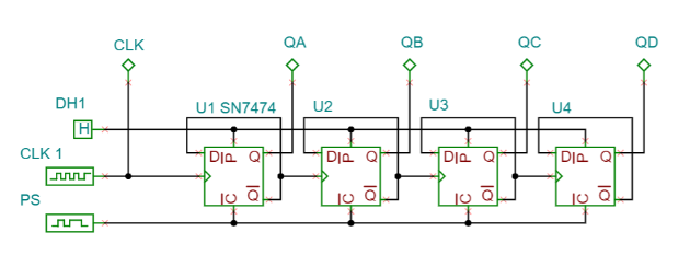
The least significant bit is QA. The clock source is 1Hz for good interactivity. Following the practice, we assign a short clear pulse by PS at the very beginning before the counting sequence to reset the flip-flops. The full name of the circuit is “asynchronous binary up counter”. Asynchronous, because each flip-flop has a distinctive clock, usually from the previous stage.

Press the Transient Interactive button. As we can see when the clock is changing low to high the indicator turns red, then the least significant flip-flop, U1, will toggle, and this effect propagates through each flip-flop.

This ripple phenomenon causes a delay in the nanosecond domain, but if we don’t care about an immediate result, short transients are acceptable.

Inserting a Prescaler

Before testing our circuit in a real FPGA environment, we need to extend our schematic with FPGA pin connectors.

Since the board doesn’t provide a 1Hz clock, we have to apply a Prescaler which will produce that from the DE10-Lite 50MHz oscillator.

The PreScaler macro has one input named “Clk” and one output named “PClk”.
The clock frequency at Clk input is 100MHz, and it is 1Hz at the PClk output by default.

The Prescaler itself is also a counter. When the counter reaches 25,000,000, the PClk output is toggled so that the frequency of the clock at this output is 1Hz. This is an additional logic to reach slow, human readable operation speed.

The simulation of this circuit must be handled with care. Because the Prescaler has to count to a very large number before the output toggles, we have to slow down this module therefore in the simulation.

Using a Push button

Replace the Clock Source with a Push button.

Let the Push button (PB) generate a high level, when it is pressed and a low level when it is at rest. When the button is pressed, a rising edge occurs on the clock input of the first flip-flop, and the counter outputs will produce the next binary code.

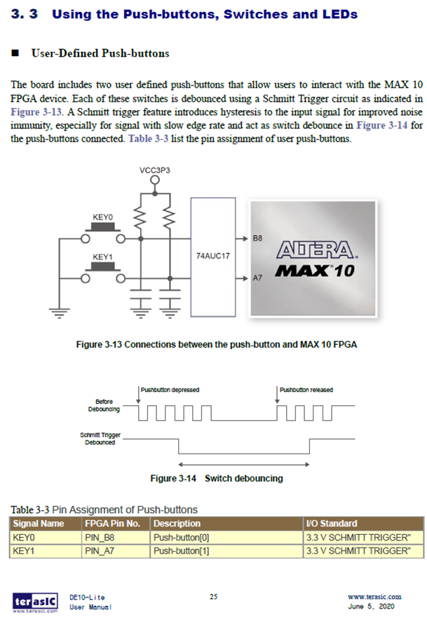
If we press a button once in the real world that may generate a series of pulses. To debounce the buttons, either FPGA logic or external circuit is necessary.

The Terasic FPGA board will eliminate the unwanted glitches by a Schmitt trigger circuit constructing a single low pulse when the button is pressed.

User-defined Push-buttons (DE10-Lite User Manual)


Modifying the circuit for using these buttons

Remove the Push button and the Resistor. These are not necessary because they are on the board and don’t belong to the synthesizable logic. Remove the Pulse Source as well.

The KEY0 button will be connected to the Clear input of the flip-flops, while KEY1 will provide the Clock.

Since we will not need the Logic Indicators we can delete them.

The circuit is ready for the export of Intel Quartus.

Here every time the KEY1 is pressed and released a rising edge is applied to the counter clock input and as a result it counts up by one.

If we press KEY0 then the counter outputs go to zero.

To watch our video click  here.

You can learn more about TINA here: www.tina.com

You can learn more about TINACloud here: www.tinacloud.com

Programming a Terasic Intel FPGA board in Verilog with TINACloud

Programming a Terasic Intel FPGA board in Verilog with TINACloud

In our other videos we have shown how you can create a digital circuit and download to an FPGA board by using TINACloud’s Schematic Editor:
Programming a Terasic Intel FPGA board with TINACloud using Schematic Design Entry and the VHDL hardware description language:
Programming a Terasic Intel FPGA board in VHDL with TINACloud.

Now, in this video tutorial our circuit, a full adder will be based on the Verilog hardware description language.

The textual description of the hardware greatly enhances portability and reusability.
By using hardware description languages describing the fundamental operations, structures and connections, virtually any logical circuit can be defined.

As we stated earlier TINACloud works with schematics, but we can also place HDL macros, including VHDL and Verilog, in the design.

First, we will test our circuit with Verilog circuit simulation in TINACloud.

The circuit operates like a half adder while Carry_In value is low.
  • When both inputs are low while Carry_In is also low, then Sum and Carry_Out are also low.
  • When just one input is low while Carry_In is low, then Sum is high and Carry_Out is also low.
  • When both inputs are high when Carry_In is low, then Sum is low and Carry_Out is high.
Now, let’s see what happens when Carry_In is high.
  • When Carry_In is high while both inputs are low, then Sum is high too and Carry_Out is low.
  • When Carry_In is high while only one input is high, then Sum is low and Carry_Out is also high.
  • When Carry_In is high while both inputs are high, then Sum and Carry_Out are also high.

If Carry_in is high, then the output values change as if we had added one to the full adder.

Next, we will export the Verilog to the Intel Quartus software, compile it and load the resulting bitstream into the Terasic DE10-Lite Intel FPGA board.

Finally, we will present how our simulated full adder circuit works along with the programmed Terasic DE10-Lite hardware and show  that in all cases, the results are exactly the same.

Check our other video “Programming a Terasic Intel FPGA Board in VHDL with TINACloud”, where we use a Verilog component in FPGA design.

To learn more please click  here.

You can learn more about TINA here: www.tina.com

You can learn more about TINACloud here: www.tinacloud.com

Programming a Terasic Intel FPGA board in VHDL with TINACloud

Programming a Terasic Intel FPGA board in VHDL with TINACloud

In our other videos, we have shown how you can create a digital circuit and download to an FPGA board by using TINACloud’s Schematic Editor: (Programming a Terasic Intel FPGA board with TINACloud using Schematic Design Entry)

and the Verilog hardware description language: (Programming a Terasic Intel FPGA board in Verilog with TINACloud).

Now, in this video tutorial, our circuit, a full adder, will be based on the VHDL hardware description language.

As we stated earlier, TINACloud works with schematics, but we can also place HDL macros, including VHDL and Verilog, in the design.  

Now, let’s see an example, a full adder using the half-adder VHDL macros.

Start TINACloud, then open the Full_Adder_VHDL_DE10-Lite.TSC from the TINA Examples\FPGA folder.

Most digital circuits that perform addition or subtraction use full adder. This combinational circuit adds two binary digits and a carry-in to produce a sum and carry-out. This one-bit full-adder cell has three inputs (A, B, Carry_In) and two outputs (Sum, Carry_Out) by applying a half adder to accept the carry-in (Carry_In) input from the previous less-significant stage of a multiple bit adder. 

The circuit operates like a half adder while the Carry-In value is low. 

Start the simulation by pressing the Dig Interactive button. 

  • When both inputs are low while Carry_In is also low, then Sum and Carry_Out are also low. 
  • When just one input is low while Carry_In is low, then Sum is high and Carry_Out is also low. 
  • When both inputs are high when Carry_In is low, then Sum is low and Carry_Out is high.

Now, let’s see what happens when Carry_In is high.

  • When Carry_In is High while both inputs are low, then Sum is high too and Carry_Out is low. 
  • When Carry_In is High while only one input is high then Sum is low and Carry_Out is also high. 
  • When Carry_In is High while both inputs are high then Sum and Carry_Out are also high. 
If Carry_In is high, then the output values change as if we have added one to the full adder. 

In the following we will test our circuit in a real environment using the Terasic DE10-Lite Intel FPGA Trainer Board. 

As it can be seen, this circuit is already prepared for the FPGA Tool export. 

(See our previous video: (Programming a Terasic Intel FPGA board with TINACloud using Schematic Design Entry)

In the following we will show how to  generate the source file for Intel Quartus Prime Lite.

Finally we will present how our simulated full adder circuit works along with the programmed Terasic DE10-Lite hardware.

As you can see, in all cases, the results are exactly the same.

This is a great example of demonstrating the power of simulation, since you can test and debug circuits even before realizing them, and in our case before downloading to FPGA, where if there were any issues, it would be extremely hard to find the problem.

Check our other video “Programming a Terasic Intel FPGA Board in Verilog with TINACloud”, where we use a Verilog component in FPGA design.

To learn more please click  here.

You can learn more about TINA here: www.tina.com

You can learn more about TINACloud here: www.tinacloud.com

Programming a Terasic Intel FPGA board in Verilog with TINA

Programming a Terasic Intel FPGA board in Verilog with TINA

In our other videos we have shown how you can create a digital circuit and download to an FPGA board by using TINA’s Schematic Editor:
Programming a Terasic Intel FPGA board with TINA using Schematic Design Entry and the VHDL hardware description language:
Programming a Terasic Intel FPGA board in VHDL with TINA
.

Now, in this video tutorial our circuit, a full adder will be based on the Verilog hardware description language.

The textual description of the hardware greatly enhances portability and reusability.
By using hardware description languages describing the fundamental operations, structures and connections, virtually any logical circuit can be defined.

As we stated earlier TINA works with schematics, but we can also place HDL macros, including VHDL and Verilog, in the design.

First, we will test our circuit with Verilog circuit simulation in TINA.

The circuit operates like a half adder while Carry_In value is low.
  • When both inputs are low while Carry_In is also low, then Sum and Carry_Out are also low.
  • When just one input is low while Carry_In is low, then Sum is high and Carry_Out is also low.
  • When both inputs are high when Carry_In is low, then Sum is low and Carry_Out is high.
Now, let’s see what happens when Carry_In is high.
  • When Carry_In is high while both inputs are low, then Sum is high too and Carry_Out is low.
  • When Carry_In is high while only one input is high, then Sum is low and Carry_Out is also high.
  • When Carry_In is high while both inputs are high, then Sum and Carry_Out are also high.

If Carry_in is high, then the output values change as if we had added one to the full adder.

Next, we will export the Verilog to the Intel Quartus software, compile it and load the resulting bitstream into the Terasic DE10-Lite Intel FPGA board.

Finally, we will present how our simulated full adder circuit works along with the programmed Terasic DE10-Lite hardware and show  that in all cases, the results are exactly the same.

Check our other video “Programming a Terasic Intel FPGA Board in VHDL with TINA”, where we use a Verilog component in FPGA design.

To learn more please click  here.

You can learn more about TINA here: www.tina.com

You can learn more about TINACloud here: www.tinacloud.com