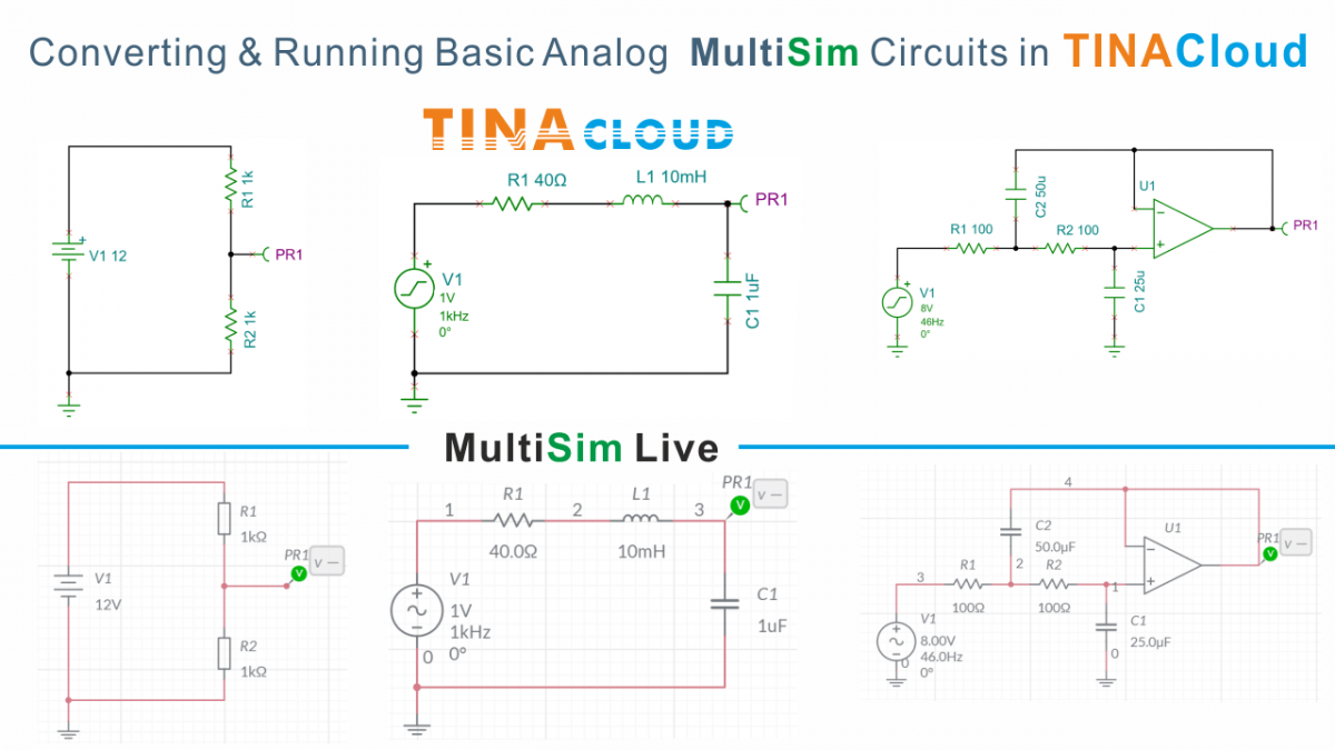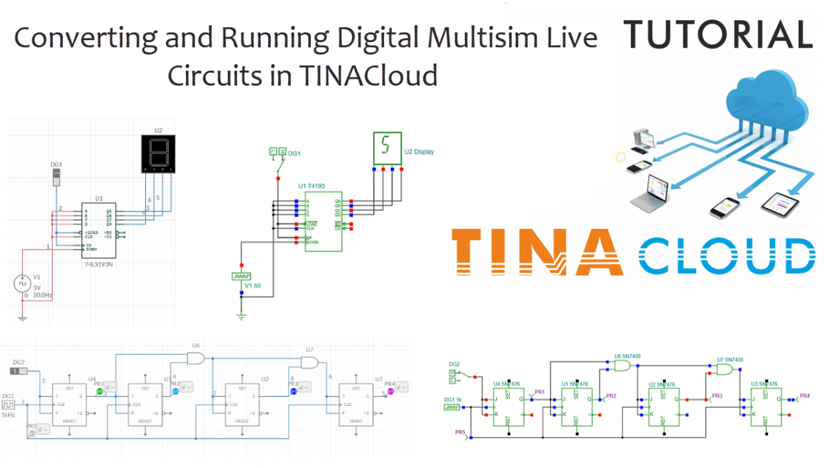
In this post, we demonstrate how to seamlessly convert and run digital circuits from Multisim Live using TINACloud.
This feature of TINACloud and TINA is especially valuable because Multisim Live does not currently support the conversion of digital circuits into the .MS14 format, which limits their use in the offline Multisim environment. TINA ensures a seamless conversion of any .MSJS format files, allowing for the simulation of converted circuits in both TINACloud and the offline TINA environment.
Click here or on the image above to watch this blog presented as a video tutorial.
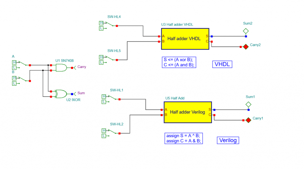
Example 1: Half Adder Circuit
We will begin with a Half Adder circuit, which we have already downloaded to our hard drive. To start, simply open the file in TINACloud using the Upload command.
Testing the Digital Circuit
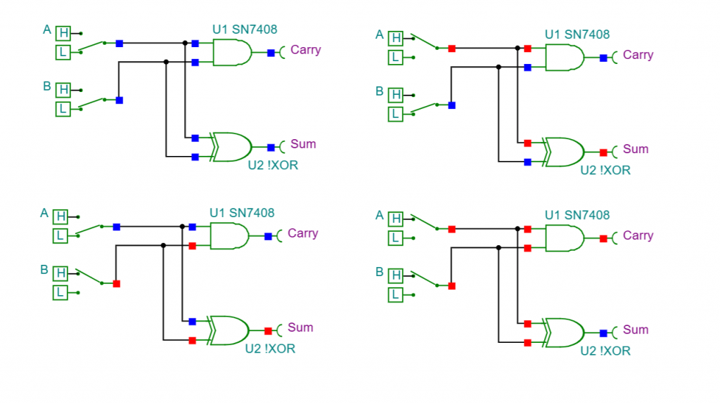
Once the circuit appears in TINACloud, we can begin testing. A great feature of TINACloud is its ability to display digital states—not just on the output, but on any visible digital node on the screen.
- Change Switch A to High: You will see the state change at the Sum output.
- Change Switch B to High: It again appears at the Sum.
- Both Inputs High: If both A and B switches are ON, the Sum becomes zero (Low) and the Carry becomes High. This confirms the standard operation of a Half Adder.
VHDL and Verilog Subcircuits
TINACloud and TINA also allow digital circuits to be modeled using Hardware Description Languages (HDLs) like VHDL and Verilog. These descriptions are essential in modern electronics as they can be synthesized into FPGAs.
To demonstrate, we added two subcircuits: the Half Adder VHDL and Verilog macros. You can view the code by double-clicking the Macro, going to Properties, and clicking the three dots (Details) on the HDL line.
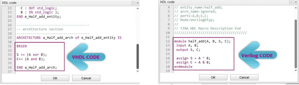
Today, it is very common to describe digital circuits using HDL code instead of building them from individual logic gates. Hardware description languages such as VHDL and Verilog allow designers to work at a higher level of abstraction, making development faster and more efficient. While this example is simple, the same approach is used for designing much more complex digital systems.
For more information on creating and uploading digital circuits to Xilinx and Intel FPGA boards using VHDL, Verilog, or schematic designs, visit our YouTube channel: https://www.youtube.com/@TinaDesignSuite
Comparing Results
In TINACloud’s Interactive Digital Mode, you can see that the VHDL and Verilog macros produce the exact same results as the original gate-level circuit. Whether using one input or both, the Sum and Carry outputs match perfectly. Using HDL allows designers to work at a higher level of abstraction, making development faster and more efficient for complex systems.
Example 2: Analyzing a 4-Bit Digital Counter
1. Circuit Import
Our next example is a 4-bit digital counter composed of four JK flip-flops. We convert the Multisim circuit into TINACloud using the standard import process, and the schematic appears directly on the workspace.
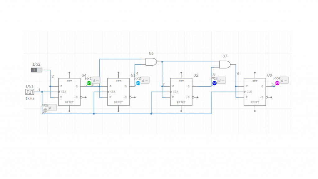
2. Interactive Simulation
By clicking the DIG button, you can observe the signal propagating through each flip-flop until it reaches the final PR4 output.
3. Digital Analysis & Timing Diagrams
To get a clearer picture of high-speed operations, we can generate a timing diagram:
- Navigate to the Analysis menu and select Digital.
- Set the analysis time to 20 milliseconds.
- Click Run.
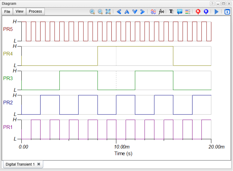
4. Frequency Division Results
The waveforms clearly demonstrate binary counting behavior:
- PR5 (Input Clock): The base high-frequency signal.
- PR1 (First Stage): Frequency is half of the input.
- PR2 (Second Stage): Frequency is one-fourth of the input.
- PR3 (Third Stage): Frequency is 1/8th of the input.
- PR4 (Final Stage): Frequency is 1/16th of the input.
The diagram confirms the binary counting behavior: each successive flip-flop stage triggers at half the previous stage’s cycle, effectively doubling the period (and halving the frequency) at every step.
This feature makes the circuit applicable as a counter. Each output represents a bit in the digital counting result: the output with half the input frequency corresponds to the least significant bit (LSB), while the output with one-sixteenth of the input frequency corresponds to the most significant bit (MSB).
Let’s add a Hex Display to the circuit to demonstrate this.
The counting result appears in hexadecimal form on the display from 0 to F, and then restarts.
Simulation of a 4-Bit digital Counter with Hexadecimal Decoding
Example 3: 74LS193 Integrated Circuit Demo
Our final example features the 74LS193 Synchronous 4-bit Binary Counter IC. This circuit is configured to count down from Hex F to zero and then reset.
Pressing the DIG button starts the interactive simulation. As the circuit decrements and reaches zero, it automatically restarts the cycle.
74LS193 Integrated Circuit: Interactive simulation in TINACloud
It is important to note that TINACloud supports all digital integrated circuits from both Multisim Live and the Multisim offline environment, as these components are native to the TINA library.
Summary
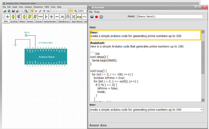
TINA and TINACloud provide a powerful bridge for your Multisim Live designs. Also beyond standard logic gates and ICs, TINA supports more than 1,400 microcontrollers, including:
- PIC, AVR, and Arduino
- 8051, HCS, and STM
- ARM, TI Tiva, TI Sitara, Infineon XMC, and ESP32
You can learn more about TINACloud here: www.tinacloud.com
Explore more content from our channel: https://www.youtube.com/@TinaDesignSuite