In this tutorial video our circuits are counters. The counter is a widely used sequential logic, where the output depends on the sequence of past inputs and a present value of the input signals.
In the case of a counter, the input signal is the clock, and the output value represents a number.
The counter circuit is usually built up with flip-flops.
Now, let’s see our first example, a binary up counter.
The counter is constructed from four, rising edge sensitive D flip-flops counting from 0 to 15. Flip-flops store the count until the next event, when the clock signal produces a low to high transition.
The least significant bit is QA. The clock source is 1Hz for good interactivity.
Following the practice, we assign a short clear pulse by PS at the very beginning before the counting sequence to reset the flip-flops.
The full name of the circuit is “asynchronous binary up counter.” Asynchronous, because each flip-flop has a distinctive clock, usually from the previous stage.
Now, press the Transient interactive button.
Let’s examine the circuit operation.
When the clock is changing low to high the indicator turns red, then the least significant flip-flop, U1, will toggle, and this effect propagates through each flip-flop. This ripple phenomenon causes a delay in the nanosecond domain, but if we don’t care about an immediate result, short transients are acceptable.
Eextending our schematic with FPGA pin connectors
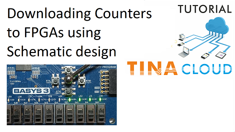
Now, before testing our circuit in a real FPGA environment, we need to extend our schematic with FPGA pin connectors as we have shown in our previous video. We will use a Digilent BASYS3 FPGA board.
We shouldn’t forget what resources our FPGA board offers. Regarding the BASYS3 board, we should note that such a board has only one clock generator with 100MHz output frequency.
Since the board doesn’t provide a 1Hz clock, we have to apply a prescaler which will produce that [PS1] from the BASYS3 100MHz oscillator.
Applying a Prescaler
Now, let’s insert this prescaler as a macro which has been written in VHDL.
Select Insert Global Macro… from the Insert menu denoted by a green plus sign, then in the Global macros dialog select the prescaler and click OK.
Place the macro on the workspace, then pan the circuit by holding down the left mouse button while moving the mouse.
Now, you can attach the macro to the input of the circuit so that the clock frequency will be divided at the input of the counter.
The prescaler macro has one input named “Clk” and one output named “PClk”.
The clock frequency at Clk input is 100MHz, and it is 1Hz at the PClk output.
The prescaler itself is also a counter. When the counter reaches 50,000,000 the PClk output is toggled so that the frequency of the clock at this output is 1Hz.
This is an additional logic to reach slow, human readable operation speed. Now, add the FPGA pin connectors to the circuit as shown next. The simulation of this circuit must be handled with care. Because the prescaler has to count to a very large number before the output toggles, we have to slow down this module.
Therefore, in the simulation, change the input clock frequency to 100Hz and change the macro code so that the counter counts up to 50 instead of 50,000,000. This way we will have a 1Hz clock coming out of the prescaler for the simulator.
Press the TR button to start the simulation.
A counter can count not only a series of pulses, but other events too. For example, the number of times a push button has been pressed .
Replacing the Clock source with a Push button
To demonstrate this, let’s go back to our original circuit.
Replace the clock source with a push button.
Let the push button (PB) generate a high level when it is pressed and a low level when it is at rest.
The low level needs a resistor.
Thus, it will work the same way as the button does on the BASYS3 board.
Start Transient interactive analysis by pressing the TR button, then click the push button (PB) to step the counter. When the button is pressed, a rising edge occurs on the clock input of the first flip-flop, and the counter outputs will produce the next binary code.
Placing a contact debouncing VHDL macro
Here, we note that the mechanical switches and push buttons have contact bouncing problems. If we press a button once in the real world, that may generate a series of pulses. That’s why we place a contact debouncing VHDL macro at the counter input.
Before we do that, remove the push button and the resistor. These are not necessary because they are on the board and don’t belong to the synthesizable logic.
Remove the pulse source, too.
The FPGA will take care of resetting the flip-flops.
Now, let’s insert the macro named “debouncer”, which has two inputs (Clk and PB) and two outputs (PBDown and PBUp).
Clk is connected to the BASYS 3 clock port, and PB is connected to the center push button (btnC) of the board. Output PBDown is connected to the clock input of the first counter flip-flop.
Click the Insert menu, then select Insert Global Macro. Select the debouncer, then click OK.
Place a Clock from the Sources Toolbar. Change its frequency to 100M and rename its label as “Clock”, then connect it to the debouncer macro. The debouncer will eliminate the unwanted glitches by resampling the button’s signal with a low frequency and constructing a single pulse when the button is pressed or released.
Place 4 more FPGA pin connectors and connect them to the Logic indicators (QA, QB, QC, QD).
Set their parameters and rename them as we did previously.
Here, every time the center push button is pressed, a pulse is sent to the counter and as a result it counts up by one.
To learn more please click here.
You can learn more about TINA here: www.tina.com
You can learn more about TINACloud here: www.tinacloud.com