Today, we are releasing an updated informational video about TINACloud, the cloud-based, multi-language version of the popular circuit simulation software TINA DesignSuite.
Universal Compatibility
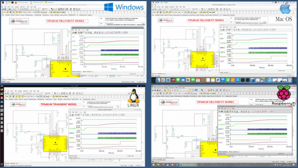
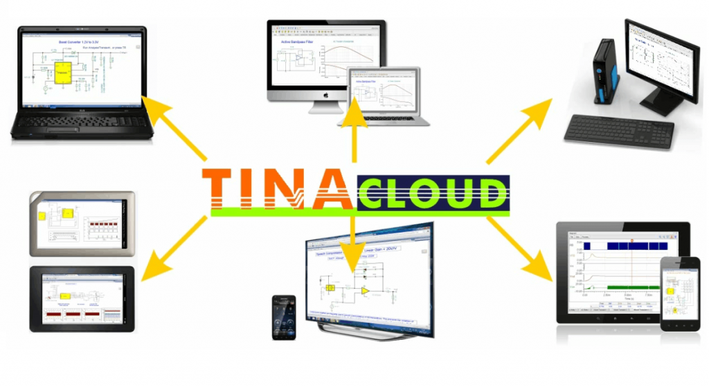
TINACloud runs on most Operating Systems including Windows, Linux, MacOS, iOS, Android and computers including PCs, Macs, thin clients, tablets, even on many smart phones, smart TVs and e-book readers.
Versatile Design and Analysis Capabilities
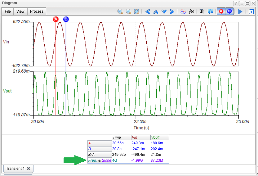
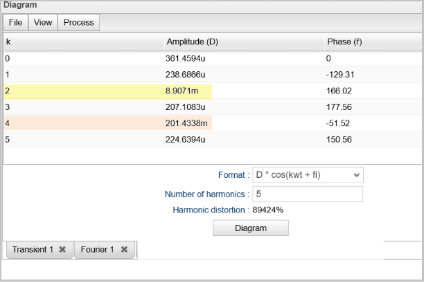
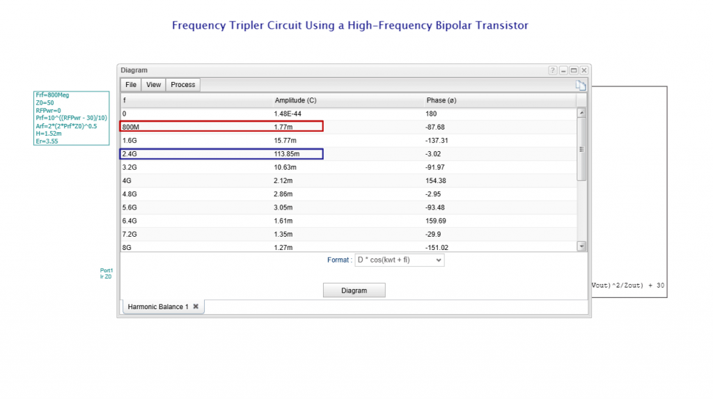
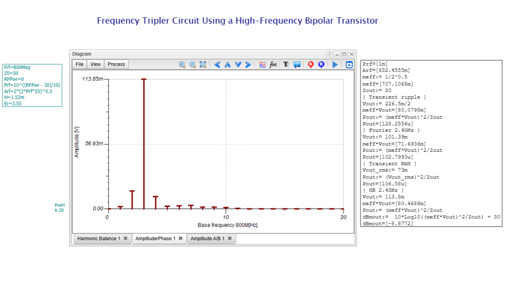
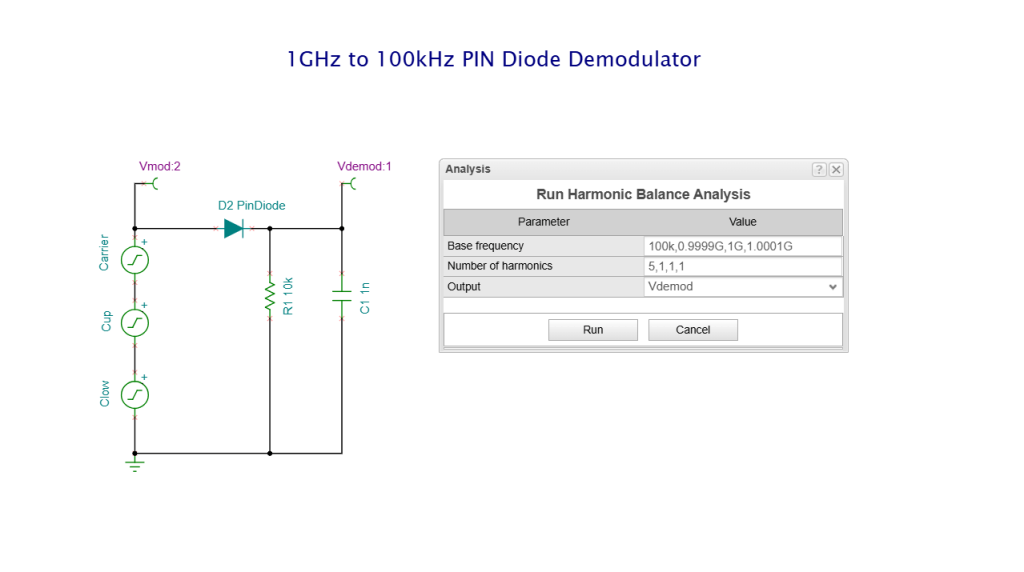
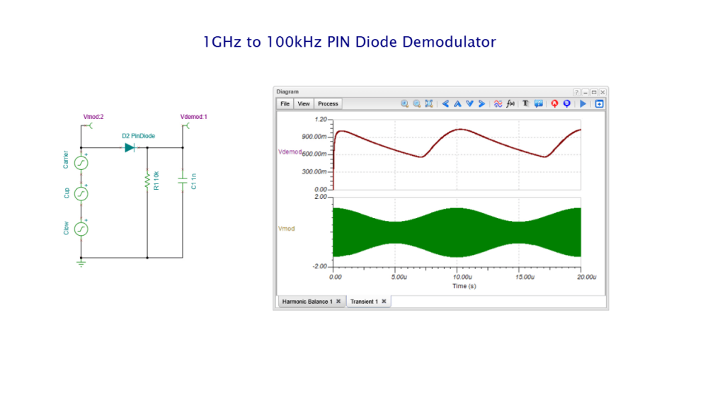
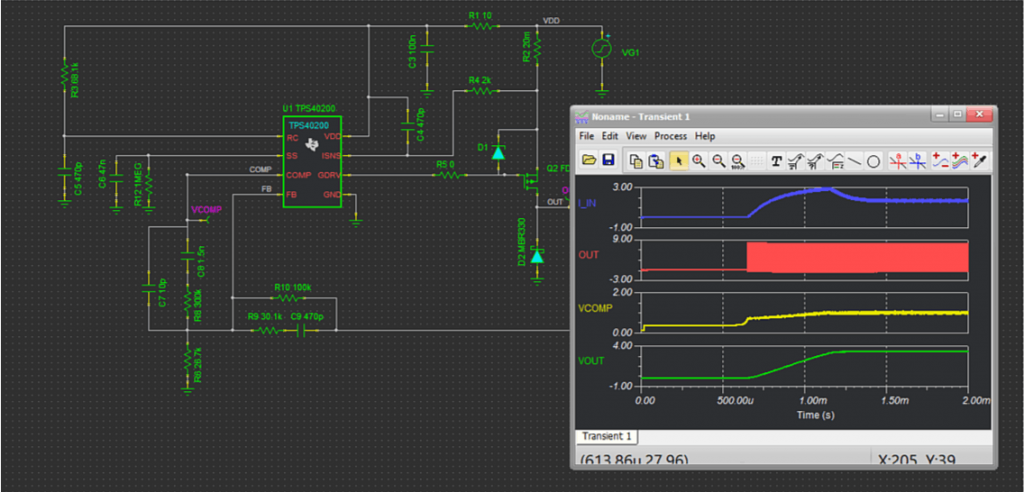
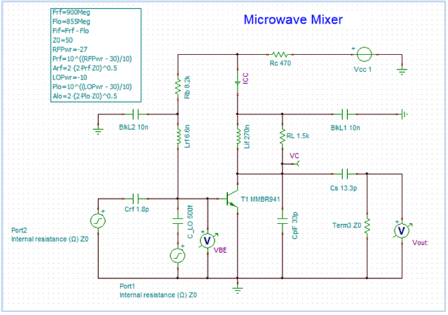
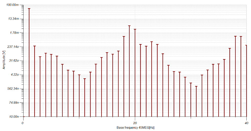
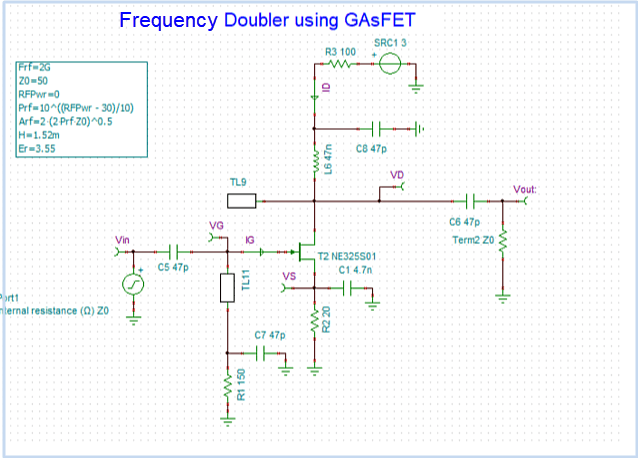
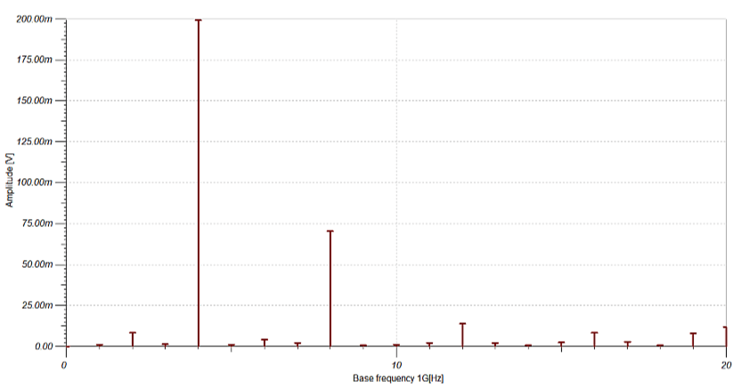
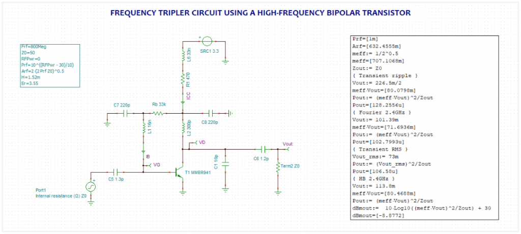
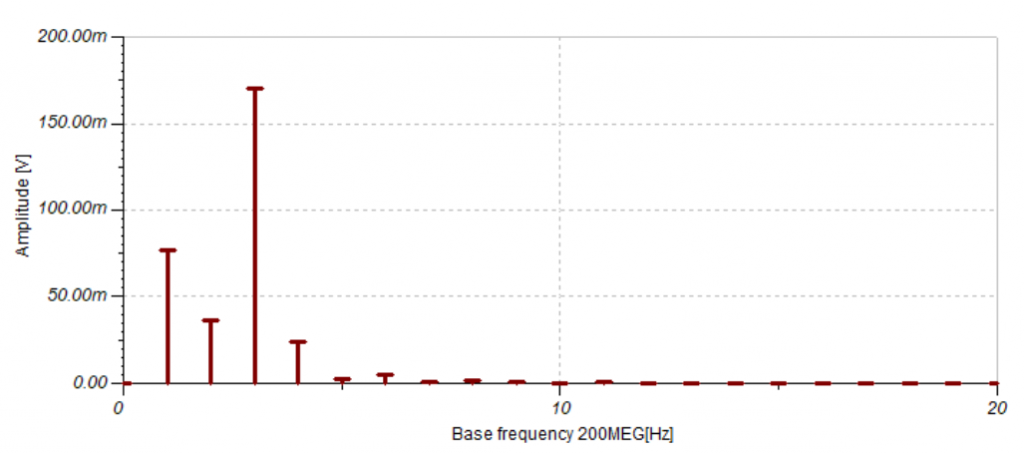
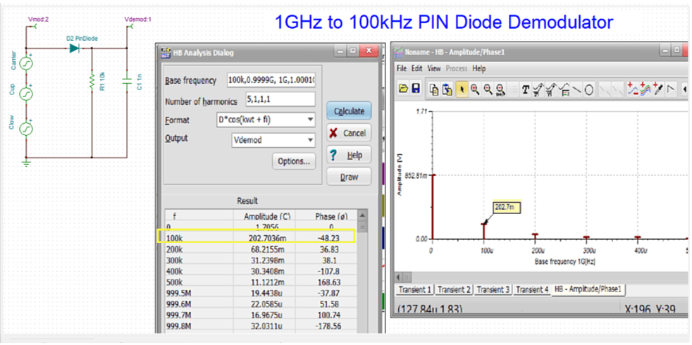
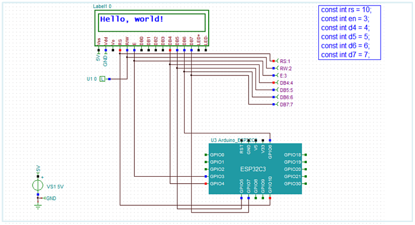
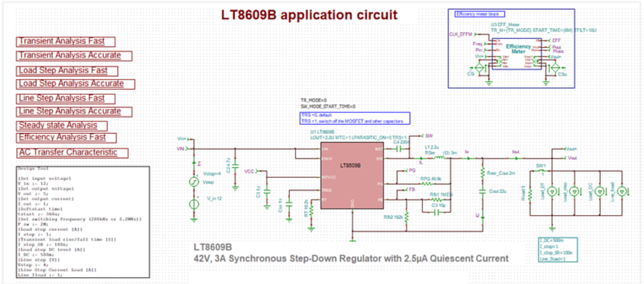
The software allows you to analyze and design a wide range of circuits, including analog, digital, Microcontroller (MCU), Switched Mode Power Supply (SMPS), Nonlinear Radio-frequency (RF), and Microwave. Recent updates now also include the popular ESP32 microcontroller family.
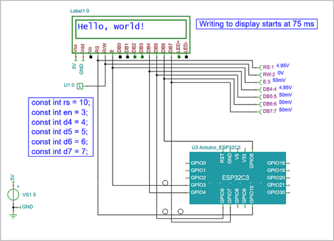
ESP32C3 microcontroller
With TINACloud, you can:
- Use manufacturer-specific SPICE models and hardware description languages.
- Test microcontroller applications in a mixed-circuit environment.
- Model complex integrated circuits such as SAR and Sigma-Delta ADCs, DAC converters with SPI, and digital power ICs with I2C and PM bus.
- Access a library of over 1400 microcontrollers, including PIC, AVR, 8051, HCS, ARM, ESP32, ST, Arduino, XMC and more.
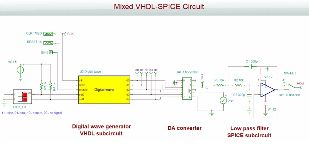
Advanced Hardware Description Languages (HDL)
In addition to SPICE, TINACloud supports five major Hardware Description Languages (VHDL, Verilog, Verilog A & AMS, and SystemC). This integration is essential for modeling modern, complex circuits in mixed-signal environments, such as:
- Mixed SPICE-VHDL and SPICE-Verilog
- Mixed SPICE-Verilog-AMS and SPICE-SystemC
AI-Powered Engineering Tools
TINACloud features integrated AI tools that provide a flexible, user-friendly interface for various engineering and educational tasks:
- Providing information on circuits
- Designing LDO and SMPS power supply circuits
- Designing active and passive filters
- Designing analog oscillators and digital clock generators
- Selecting and redesigning evaluation circuits from different manufacturers
- Generating Arduino code for rapid prototyping
- Generating complex Python code for custom analysis
- Creating step-by-step solution of simple DC/AC circuits
- Creating quizzes and riddles and check their solution
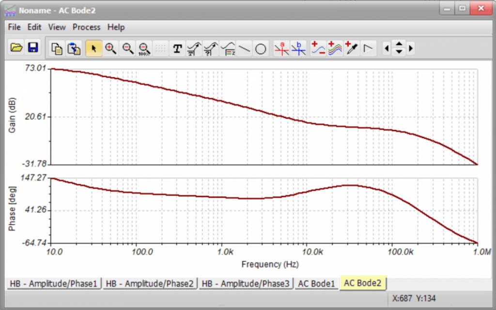
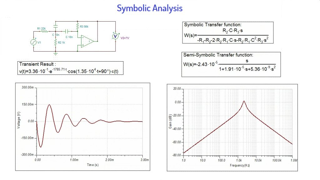
Unique Symbolic Analysis
A standout feature of TINACloud is its Symbolic Analysis capability. This produces closed-form expressions for transfer functions, equivalent resistance, and impedance.
- In DC and AC modes, it derives formulas in full or semi-symbolic forms.
- In Transient analysis, responses are determined as a function of time.
- It also allows for the calculation and plotting of poles and zeros in linear circuits, providing deeper insight than numerical analysis alone.
Integrated PCB Design
TINACloud is extended with the fully integrated TINA PCB Designer. This professional toolset includes:
- Autoplacement and autorouting.
- “Follow-me” trace placement and Design Rule Checking (DRC).
- Forward and backward annotation.
- Support for flexible PCB layouts, 3D viewing, and Gerber/G-code output.
Industry Partnership: Infineon Technologies
Since 2014, Infineon Technologies, one of the world leaders in the power electronics industry, has been using TINACloud as the engine for its online prototyping tool, Infineon Designer. TINACloud and TINA include thousands of models of Infineon’s LED drivers, high-voltage, high-power, RF, MCU and other parts, along with a large number of industrial prototypes and application circuits that can be processed and developed further in both TINA and TINA Cloud.
Conclusion
Whether you are a student, an educator, or an experienced professional in circuit design, TINA and TINACloud provide powerful, intuitive analysis—offline and online. Much more than just another SPICE program, this is software designed to help you advance your ideas, refine your products, and master the behavior of complex electronic circuits.
Content of the video:
- 00:00 Introduction to TINACloud
- 00:12 Cross-Platform Compatibility: Access on PC, Mac, tablets, and mobile
- 00:27 Circuit Design & Simulation: Analog, Digital, MCU, and RF capabilities
- 00:57 Advanced HDL Support: Integration of VHDL, Verilog, and SystemC
- 01:49 AI-Driven Design Tools for Filters, Oscillators, SMPS Design, and Code Generation
- 02:33 Symbolic Analysis: Generating closed-form expressions and transfer functions
- 03:23 Integrated PCB Designer: From schematic to layout with 3D visualization
- 04:05 Industry Partnership: TINACloud and Infineon Technologies
- 04:37 Who is TINACloud for? (Professional Designers, Educators, and Students)
- 05:35 Website Information
You can learn more about TINACloud here: www.tinacloud.com
You can learn more about TINA here: www.tina.com
Explore more content from our channel: https://www.youtube.com/@TinaDesignSuite