
In this video our counter will be based on the VHDL hardware description language.
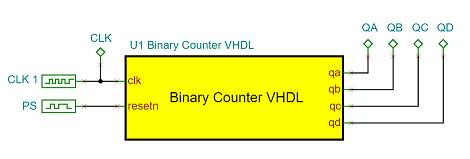
In our first example, Binary Counter VHDL circuit, we replace the flip flops by a macro which has been written in VHDL.
The macro has two inputs, one for the Clock (clk) and another for the active-low reset (resetn). Clk is connected to the Clock Source, and resetn is connected to the reset Pulse Source.
The four outputs (QA, QB, QC, QD) provide the counter value.
The Binary Counter entity has the same inputs and outputs as the macro shape.
simulation of the binary counter vhdl circuit
Binary Counter VHDL circuit
We can start the simulation by pressing the Transient Interactive button.
When the clock is changing low to high the indicator turns red then the QA, the least significant bit, toggles. Then, at each rising edge of the clock, the count value goes up by one.
When the Counter reaches the maximum value (binary 1111), the output goes zero.
testing our circuit with the Terasic de10-Lite FPGA board
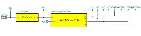
Before testing our circuit in a real FPGA environment, we need to extend our schematic with FPGA pin connectors. Since the board doesn’t provide a one hertz Clock, we have to apply a Prescaler which will produce that from the DE10-Lite 50 MHz Oscillator.
The prescaler macro has one input named clk and one output named pclk. The clock frequency at clk input is 100 megahertz and it is one hertz at the pclk output by default. To adjust the VHDL code to the board 50 MHz frequency, we modify the ‘Presc < 50000000’ expression constant to 25 million in the Prescaler macro.
The prescaler itself is also a counter. When the counter reaches 25 million the PClk output is toggled, so that the frequency of the clock at this output is 1Hz.
Next, we will place the FPGA Pin connectors. We will attach the first Pin connector to the Clock input before the Prescaler . Then, we will connect 4 more FPGA pin connectors to the 4 outputs of the circuit and assign them to the LEDs: LEDR[0], LEDR[1], LEDR[2] and LEDR[3] .
The counter will be initialized by the FPGA automatically before generating the source files for Intel Quartus-Lite.
Generating the source files for Intel Quartus-Lite.
First we will add the sources files, the VHDL and the QSF files. The VHDL file is the top-level entity wrapping the underlying components and connections around. The content of the QSF file will tell the software which FPGA pins are to be used for the logic inputs and outputs.
Next, we will compile the files for the FPGA.
As soon as the “Full Compilation was successful” message appears, we will program the device.
You will see the “Progress bar at 100%, successful” message and also you will see the counter lights come up counting up in binary.
If the output code reaches the maximum value of 15 the counter next state will be zero.
replacing the clock source with a push button
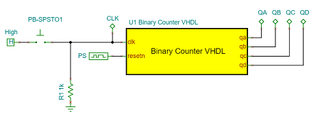
A counter can count not only a series of pulses but other events too. For example the number of times a push button has been pressed.
To demonstrate this, we will return to our original circuit and replace the the Clock Source with a Push Button. Let the push button PB generate a high level when it is pressed and a low level when it is at rest.
We will also place a Resistor and a Digital High Source. No, we can start the simulation by pressing the TR button. When the button is pressed a rising edge occurs on the clock input of binary counter entity and the counter outputs will produce the next binary code.
implementing this circuit in a real fpga environment using the Terasic DE10-Lite board
First we will remove the Push button, the Resistor and the Pulse Source. Next, we will place 2 FPGA Pin Connectors named as KEY0 and KEY1.
The KEY0 button will be connected to the resetn input of the counter, while KEY1 will provide the clock. We will place four more Pin Connectors and connect them to the Logic Indicators QA, QB, QC, QD. Then we will set their parameters as we did previously: LEDR[0], LEDR[1], LEDR[2] and LEDR[3].
Since we will not need the Logic Indicators we can delete them now.
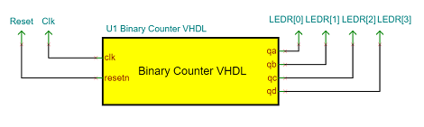
Every time the KEY1 is pressed and released a rising edge is applied to the counter clock input and as a result it counts up by one.
If we press KEY0 then the Counter outputs go to zero.
To watch our video click here.
You can learn more about TINA here: www.tina.com
You can learn more about TINACloud here: www.tinacloud.com