In this video, first, we will demonstrate how to simulate and synthesize a circuit displaying prime numbers using a PIC MCU VHDL code.
In the end, we will download the circuit’s configuration file to the Digilent Basys 3 FPGA board.
In our circuit, PIC16F84_Prime_number_generator, the PIC MCU model is written in VHDL. The VHDL code is the functional model of a PIC16F84 8-bit microcontroller with initialized flash program memory.
Looking at the VHDL code in TINA HDL editor
First, we look at the VHDL code using TINA HDL Editor.
The top-level entity is rtl_pic.
In the architecture section bound to the rtl_pic entity (line 1828), we instantiate and connect the main components.
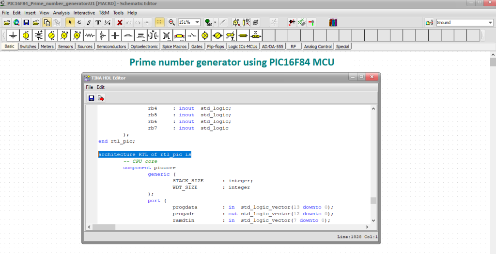
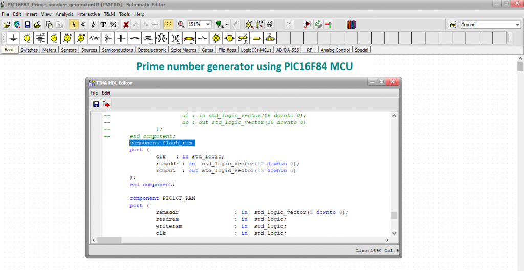
These components are the pic_core (line 1830), the 1k*14 bits flash_rom (line 1890), and the PIC16F_RAM file register (line 1898).
From line 1941, the instantiation statements connect these declared components to signals in the architecture (1941–2002), followed by auxiliary VHDL code to support reset and IO updates.
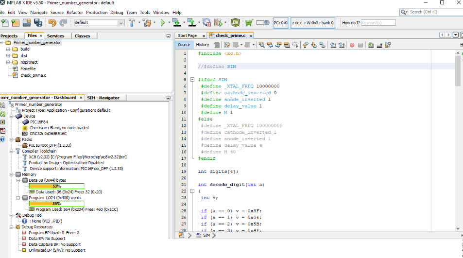
Looking at the C code in the MPLAB editor
Next, we will check the program code, written in C and converted to this VHDL code.
The project was created, and the program was developed with the free version of Microchip MPLAB IDE and their Microchip XC8 compiler.
Let’s open the MPLAB editor.
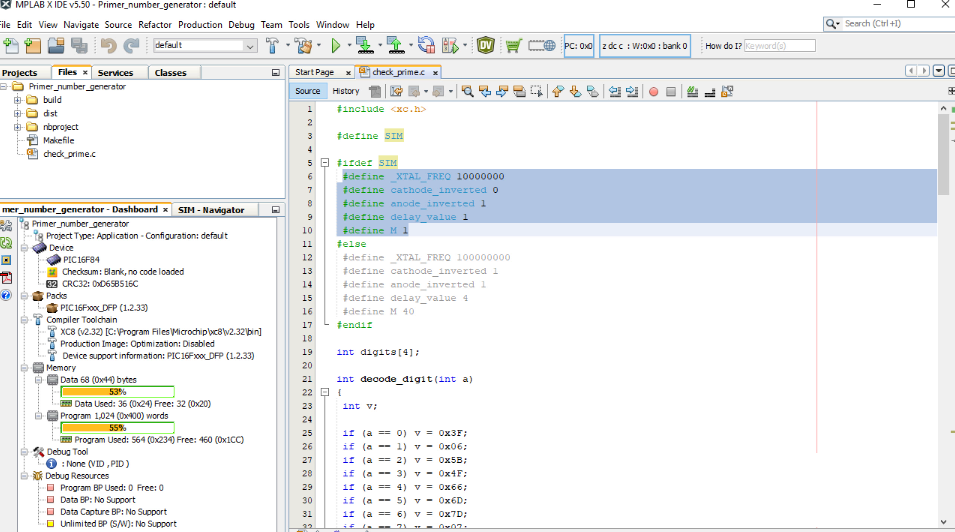
MPLAB editor
First, we define SIM, indicating that we are running a simulation (line 3).
If SIM is defined, then other constants are created in lines 6–10.
The XTAL FREQ is the processor frequency for the simulation.
The other parameters are for handling the display.
The code writes prime numbers between 1 and 9999 with the help of a for loop starting from line 98.
If a number is prime, we will generate the digits and display the number.
We have 8 bits to write a digit (PORTB) and 4 bits (PORTA) to select which one to display.
One digit is displayed for a very short time in the millisecond domain.
When a digit is displayed, the other digits are dark. This process is performed from line 107.
Circuit simulation
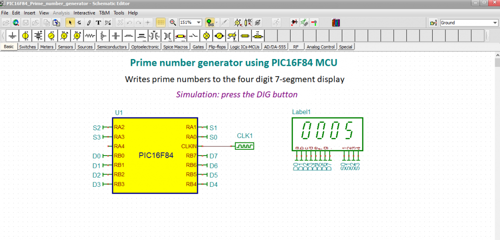
Prime number generator circuit. Circuit simulation
After that, we return to TINA’s Schematic Editor to run digital simulation. Then we go back to the MPLAB editor to make the main difference in the C code for the synthesis, like the processor speed (100 MHz). This is the oscillator frequency of the BASYS3 FPGA board. Next, we compile the project and convert the result – the executable binary – into VHDL.
MBLAB editor. Comment the SIM definition
The code is placed in the flash ROM component of our VHDL PIC model.
Testing our circuit in a real environment
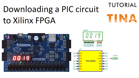
Finally, we will test our circuit, ” PIC16F84_Prime_number_generator_BASYS3” in a real environment using the Digilent BASYS3 FPGA board.
As expected, we can see the prime numbers written on the display.
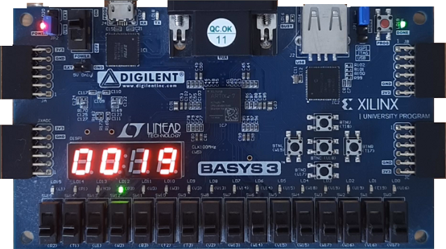
Testing the circuit in a real environment using the Digilent Basys 3 FPGA board
To watch our video click here.
You can learn more about TINA here: www.tina.com
You can learn more about TINACloud here: www.tinacloud.com