
The counter is a widely used sequential logic where the output depends on the sequence of past inputs and a present value of the input signals. In the case of a counter the input signal is the clock and the output’s value represents a number. The counter circuit is usually built up with flip flops.
Now, in this video our counter will be based on the Verilog hardware description language. The textual description of the hardware greatly enhances portability and reusability.
In our first exemple, Binary Counter Verilog.tsc we will replace the flip-flops by a macro.
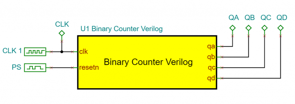
Binary Couner Verilog circuit
Let’s examine the Macro
The macro has two inputs, one for the Clock (clk) and another for the active-low reset (resetn). Clk is connected to the Clock source, and resetn is connected to the reset Pulse Source.
The four outputs (QA, AB, QC, QD) provide the counter value.
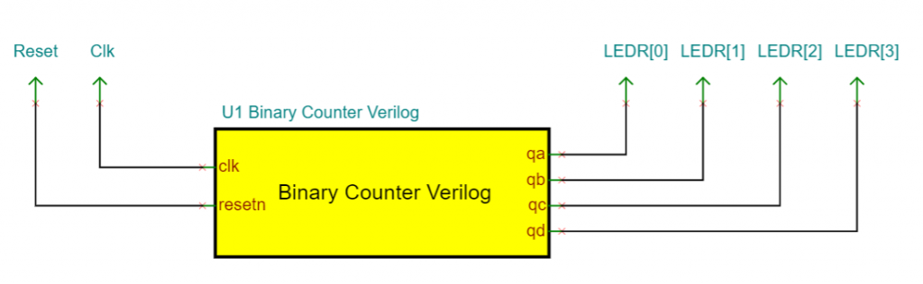
The Binary Counter module has the same inputs and outputs as the macro shape.
The always block is executed when the clock rising from low to high or the resetn input falling from high to low.
Instead of implementing a counter with flip flop inference, we increment the q register if the reset is held high and the Clk is rising. Therefore, the counter counts the Clk rising edges.
If the resetn is low then the q is reset to the value of zero.
The q register bit values are assigned to qa, qb, qc, qd respectively.
Each output line represents a binary digit.
The Clock source is one hertz for good interactivity. Following the practice, we assign a short clear pulse by PS at the very beginning before the counting sequence to reset the counter.
Let’s start the Transient analysis and examine the circuit operation
When the clock is changing low to high the indicator turns red then the qa, the least significant bit, toggles. Then, at each rising edge of the clock, the count value goes up by one.
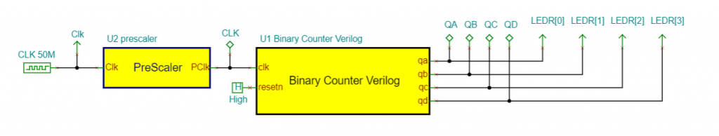
When the counter reaches the maximum value (binary 1111), the output goes zero. Now before testing our circuit in a real FPGA environment we need to extend our schematic with FPGA pin connectors. We will use a Terasic DE10-Lite Intel FPGA board.
Extending the Schematic with FPGA Pin connectors.
Regarding the DE10-Lite board we should note that such a board has clock generators with 50 megahertz output frequency.
Since the board doesn’t provide a one hertz clock, we have to apply a Prescaler which will produce that from the DE10-Lite 50 MHertz oscillator.
The prescaler macro has one input named Clk and one output named PClk. The Clock frequency at Clk input is 100 megahertz and it is one hertz at the PClk output by default. To adjust the VHDL code to the board 50 megahertz frequency, double-click the Prescaler macro, then in the properties window click the three dots at the end of the HDL code field. Modify the ‘Presc < 50000000’ expression constant to 25 million, then save by pressing OK.
The prescaler itself is also a counter. When the counter reaches 25 million the PClk output is toggled, so that the frequency of the clock at this output is one hertz. This is an additional logic to reach slow human readable operation speed.
Inserting a prescaler
Binary Counter Verilog PClk DE10-Lite circuit
Now let’s insert this Prescaler as a macro which has been written in VHDL. In TINACloud, you can mix VHDL and Verilog.
Next double-click the pin connector then in the properties window click the three dots at the end of the Pin settings field. In the Device section click the Terasic DE10-Lite, then select CLOCK under the Group section and MAX10_CLK1_50 under the Pin section.
Click ok to accept the settings. Rename the label of pin one as Clk as well and click ok.
Now, insert the FPGA pin connectors for the four outputs of the circuit and assign them to the LEDs: LEDR[0] LEDR[1] LEDR[2] and LEDR[3]. Set the LED names to LEDR[0] LEDR[1] LEDR[2] and LEDR[3] respectively.
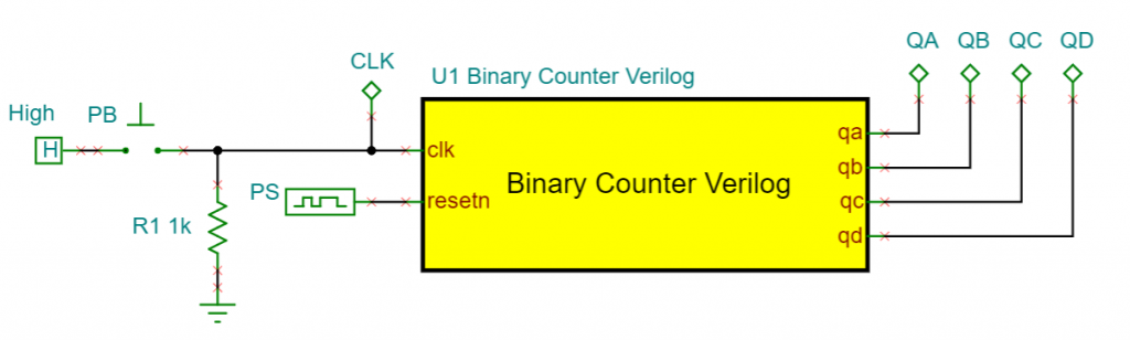
Finally remove the Pulse Source, then select a Digital High Source from the Sources Toolbar and connect it to the resetn input. Next, rename its laber as High.
A reset pulse will be assigned by the FPGA automatically.
Now, let’s generate the source files for Intel Quartus-Lite.
As soon as the “Quartus Prime Full Compilation was successful” message appears, right-click the Program Device, then click Open.
Click the Start button to program the device.
You will see the “Progress bar at 100%, successful” message and the counter lights come up counting up in binary.
If the output code reaches the maximum value of 15 the counter next state will be zero.
Slowing down the Prescaler and changing the Macro code
The simulation of this circuit must be handled with care because the prescaler has to count to a very large number, before the output toggles, we have to slow down this module therefore in the simulation.
Now, change the input clock frequency to 100 hertz, and change the macro code so that the counter counts up to 50 instead of 25 million. This way we will have a one hertz clock coming out of the prescaler for the simulator.
Replacing the Clock Source with a Push Button
Binary Counter Verilog Btn circuit
Binary Counter Verilog Btn circuit
Delete the Clock Source, then select a Push button from the Switches Toolbar.
The Push button (PB) will generate a high level when it is pressed and a low level when it is at rest. When the button is pressed a rising edge occurs on the clock input of binary counter module and the counter outputs will produce the next binary code.
Implementing this circuit on an FPGA
Here we note, that the mechanical switches and push buttons have contact bouncing problems. If we press a button once in the real world that may generate a series of pulses.
To debounce the buttons, either FPGA logic or external circuit is necessary.
The Terasic FPGA board will eliminate the unwanted glitches by a Schmitt trigger circuit constructing a single low pulse when the button is pressed.
Modifying the circuit for using these buttons
Binary Counter Verilog Btn DE10-Lite circuit
Binary Counter Verilog Btn DE10-Lite circuit
First, remove the push button and the resistor. These are not necessary because they are on the board and don’t belong to the synthesizable logic. Remove the pulse source and the Digital High Source as well. Now, select two FPGA pins then place them on the workspace.
The KEY0 button will be connected to the resetn input of the counter, while KEY1 will provide the clock.
For Pin2, select KEY[1], rename label to Clk.
Place four more Pin connectors and connect them to the Logic Indicators QA, QB, QC, QD. Set their parameters and rename them as we did previously.
Since we will not need the Logic Indicators we can delete them.
Now, the circuit is ready for the export of Intel Quartus.
Let’s generate the source files.
Now, connect DE10-Lite with the Quartus machine via USB.
Here every time the KEY1 is pressed and released a rising edge is applied to the counter clock input and as a result, it counts up by one.
If we press KEY0 then the counter outputs go to zero.
To watch our video click here.
You can learn more about TINA here: www.tina.com
You can learn more about TINACloud here: www.tinacloud.com