Bridge Sensor Amplifier With RFI Filter

Bridge Sensor Amplifier With RFI Filter

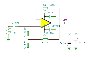
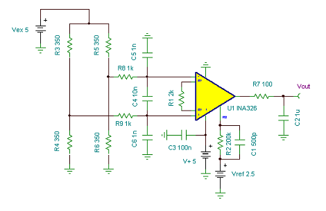
This high accuracy bridge sensor amplifier is based on the autozero INA326 instrumentation amplifier. Bridge sensors are commonly found in pressure transducers, weigh scales, strain guages, and load cells. As shown, the amplifier gain is 200V/V. Capacitors C1 & C2 form a 2nd order 1kHz low- pass filter to reduce noise. The INA326 is virtually free of 1/f noise. R8 & R9 together with C4, C5, & C6 form an RFI filter. For best filtering, make R8 = R9 and C5 = C6 as close as possible. C4 = C5 * 10. In battery- operated applications, an INA327 with shutdown is recommended. For operation over -40C to +125C, use an INA337. (Circuit is created by Neil P. Albaugh,  TI-Tucson)

The “Bridge Sensor Amplifier With RFI Filter” circuit:
Bridge Sensor Amplifier With RFI Filter
Online Simulation of the “Bridge Sensor Amplifier With RFI Filter” Circuit

The great feature of the TINA circuit simulator that you can analyze this circuit immediately with TINACloud the online version of TINA. Of course you can also run this circuit in the off-line version of TINA.

Click here to invoke TINACloud and analyze the circuit, or watch our tutorial video! 

You can send this link to any TINACloud customers and they can immediatelly load it by a single click and then run using TINACloud.

Michael Koltai
www.tina.com

INA154 With Gain-Current Shunt Amplifier

INA154 With Gain-Current Shunt Amplifier

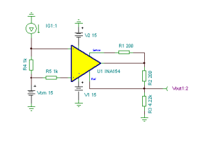
By converting the difference amplifier output to a current source using R2, voltage gain can be achieved with R3. R2 compensates the current sensing resistor R2 and increases the current source output impedance. Resistor R5 compensates for the current shunt resistance R4. Perfect compensation for R4 is not possible since the INA154’s internal resistor network is trimmed for precise ratios rather than absolute  values. A buffer amplifier should be used on the output to prevent gain (loading) error. Bypass capacitors are not shown.  (Circuit is created by Neil P. Albaugh,  TI-Tucson)

INA154 With Gain-Current Shunt Amplifier circuit:
INA154 With Gain-Current Shunt Amplifier circuit
Online Simulation of the “INA154 With Gain-Current Shunt Amplifier” Circuit

The great feature of the TINA circuit simulator that you can analyze this circuit immediately with TINACloud the online version of TINA. Of course you can also run this circuit in the off-line version of TINA.

Click here to invoke TINACloud and analyze the circuit, or watch our tutorial video! 

You can send this link to any TINACloud customers and they can immediatelly load it by a single click and then run using TINACloud.

Michael Koltai
www.tina.com
Single Supply Absolute Value Amplifier (2)

Single Supply Absolute Value Amplifier (2)
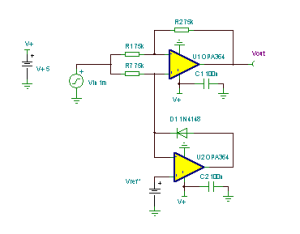
The rail- to- rail input and output characteristics of these CMOS op amps allow them to swing very close to their supply rails–+5V and ground. By forcing U1 to operate as an inverting amplifier when the input voltage is negative (by the “ideal clamp” circuit of U2 and D1) and allowing it to operate as a normal noninverting amplifier when the input voltage is positive, op amp U1 acts like a perfect rectifier. This design can be biased above ground, handy in single supply circuits referenced to V+/2. This absolute value amplifier has unity gain an input range of within a few mV of -5V to +5V. For a faster amplifier, use an OPA354 for U1 & U2 and a small Schottky diode for D1. The dual amplifier versions, OPA2364 or OPA2354 can also be used. (Circuit is created by David Jones & Neil P. Albaugh,  TI- Tucson)
Single Supply Absolute Value Amplifier (2) circuit:
Absolute-value amplifier single-supply 2
Single Supply Absolute Value Amplifier (2) circuit
Online Simulation of the “Single Supply Absolute Value Amplifier (2)” Circuit

The great feature of the TINA circuit simulator that you can analyze this circuit immediately with TINACloud the online version of TINA. Of course you can also run this circuit in the off-line version of TINA.

Click here to invoke TINACloud and analyze the circuit, or watch our tutorial video! 

You can send this link to any TINACloud customers and they can immediatelly load it by a single click and then run using TINACloud.

Michael Koltai
www.tina.com
Capacitive Load Demo

Capacitive Load Demo circuit

This “Capacitive Load Demo” circuit shows the utility of Tina- TI’s “Control Object” function. The series compensation resistor R1 is  stepped in values of 10, 30, and 50 ohms. The effect on the op amp’s overshoot is shown clearly in the plot below. Likewise, the compensation capacitor C1 or the load capacitance CL can be stepped in value and the effects evaluated. (Circuit is created by Neil P. Albaugh  TI – Tucson)

Capacitive Load Demo circuit:

Capacitive load demo-blog

Online Simulation of the “Capacitive Load Demo” Circuit

The great feature of the TINA circuit simulator that you can analyze this circuit immediately with TINACloud the online version of TINA. Of course you can also run this circuit in the off-line version of TINA.

Click here to invoke TINACloud and analyze the circuit, or watch our tutorial video!

You can send this link to any TINACloud customers and they can immediatelly load it by a single click and then run using TINACloud.

Michael Koltai
www.tina.com

Bootstrapped Input For High Impedance

Bootstrapped Input For High Impedance

Applying a small amount of positive feedback to the input bias current return resistor R3 effectively raises the apparent input resistance seen by an input signal. Without feedback the input resistance is R3 (1M) in parallel with the input resistance of U1 (1E13 ohms); positive feedback applied through the voltage divider R1 & R2 multiplies the effective input impedance of R3 by creating a smaller differential voltage across the resistor. The pole frequencies of various feedback fractions are illustrated by the AC analysis below. A piezoelectric transducer or condenser microphone is modeled by VG1 in series with capacitor C1. Without bootstrapping (positive feedback), the low- frequency cutoff is 1.8kHz but by placing a 100 ohm resistor at R1, this cut-off frequency drops to 2Hz, illustrating the increased Rin. This does not come without penalty, however. Adding bootstrapping also increases the noise gain of the op amp, multiplying its Vos, drift, and noise. Adding a LARGE capacitor in series with R1 can eliminate the amplified DC offset and drift but the low frequency noise will still suffer. Approach large + feedback fractions with caution; instability and susceptibility to external noise pickup can result. (Circuit is created by Neil P. Albaugh,  TI – Tucson)

Bootstrapped Input For High Impedance circuit:

Bootstrapped Input For High Impedance circuit
Online Simulation of the “Bootstrapped Input For High Impedance” Circuit

The great feature of the TINA circuit simulator that you can analyze this circuit immediately with TINACloud the online version of TINA. Of course you can also run this circuit in the off-line version of TINA.

Click here to invoke TINACloud and analyze the circuit, or watch our tutorial video! 

You can send this link to any TINACloud customers and they can immediatelly load it by a single click and then run using TINACloud.

Michael Koltai
www.tina.com