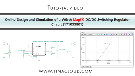
In this new video we demonstrate the online design and simulation of the Würth MagIC (171033801) DC/DC synchronous switching regulator evaluation circuit using TINACloud.
Startup Transient Simulation
The startup transient of a DC-DC converter is the period of time during which the converter is transitioning from its off state to its steady-state operating condition.
In most simulators the Startup Transient simulation takes a long time since the whole process from the initial state to steady state is simulated.
However due to the built in average model in TINA and TINACloud the simulation takes only seconds both online and offline.
TINA and TINACloud can also be used to perform switching mode transient analysis. Due to the advanced multicore solvers in both software, switching mode transient analysis is still quite fast and results in more detailed waveforms.
In addition, TINA and TINACloud include a very fast calculation of the ripple voltages using the combination of the average and switching models.
The simulation results show good agreement with the voltage measurements on the datasheet:
Comparison of simulation and measurement results
Steady State Analysis
Steady state analysis of a DC-DC power supply is the analysis of the circuit’s behavior when it has reached a steady state. This means that the output voltage is constant, except for the ripple voltage, and all the components in the circuit are operating in their steady state conditions.
TINA and TINACloud provide a very fast and accurate method for determining the ripple voltages in any circuit. They use built-in average models to quickly reach the steady state and then switching models to determine the ripple voltage.
This method allows a very fast determination of ripple voltages for any circuit settings without the need of storing initial values of inductors and capacitors in the circuits.
Line Step Analysis
Line stepping analysis of DC-DC converters is used to determine how a DC-DC converter responds to changes in the input voltage.
TINA and TINACloud can simulate the circuit response extremely fast due to their built-in average models.
Line Step Transient circuit and diagram
Load Step Analysis
Load step analysis of DC-DC converters is a type of circuit simulation that is used to determine how a DC-DC converter responds to changes in the load current.
In TINA and TINACloud you can also quickly simulate the circuit response to a load step.
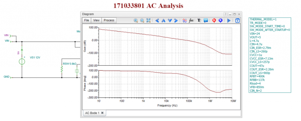
AC Analysis
The built-in average models of DC-DC converters in TINA and TINACloud allow fast and accurate AC analysis.
AC analysis is a powerful tool for designing and optimizing DC-DC converters. It provides the frequency response of the converter, which can be used to analyze its stability and performance under different conditions.
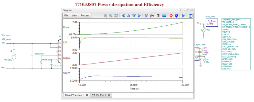
Efficiency Analysis
TINA and TINACloud also allow fast and accurate calculation of efficiency as a function of load current.
Content of the video:
- 00:00 Introduction
- 00:29 Startup Transient Simulation
- 02:11 Steady State Analysis
- 03:41 Line Stepping Analysis
- 04:14 Load Step Analysis
- 04:50 AC Analysis
- 05:27 Efficiency Analysis
- 06:00 Conclusion
Click here to watch our video.
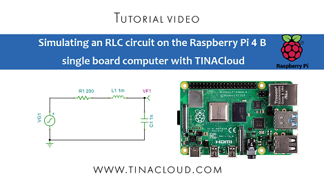
You can learn more about TINACloud here: www.tinacloud.com
You can learn more about TINA here: www.tina.com