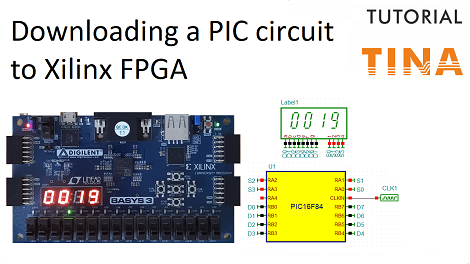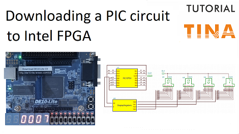
In this video, first, we will demonstrate how to simulate and synthesize a circuit displaying prime numbers using a PIC MCU VHDL code.
In the end, we will download the circuit’s configuration file to the Terasic DE10-Lite FPGA board.
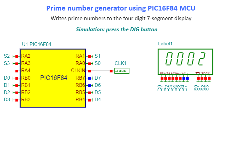
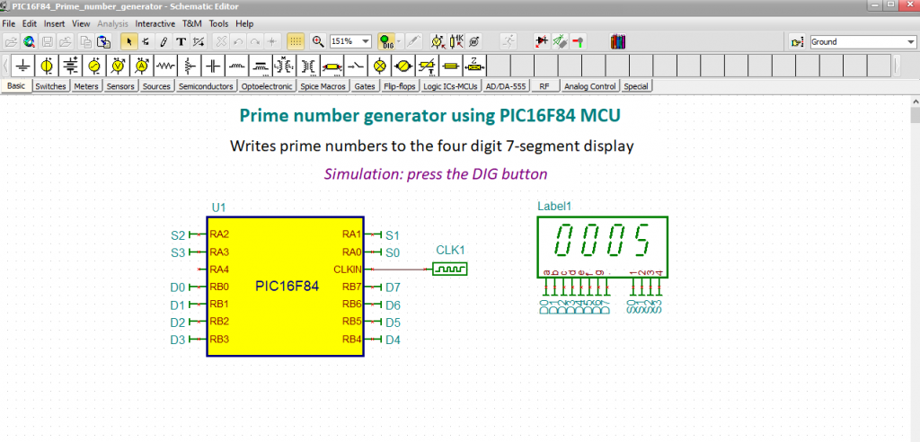
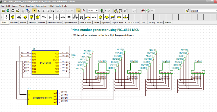
PIC16F84 Prime number generator Sim DE10 Lite circuit
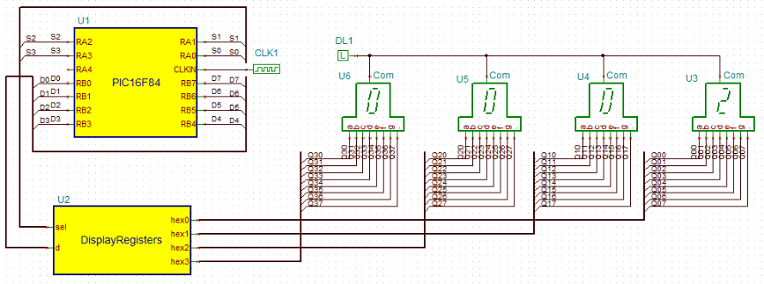
This circuit calculates prime numbers between 1 and 9999 and shows them on a 4-digit 7-segment display.
The four digits have 4 times 8, 32 pins.
Since the PIC has limited number of lines to control the display, we use an array of registers to extend its capability.
The register array is implemented in the DisplayRegisters VHDL macro.
The registers will be written by the PIC chip.
The macro has two inputs: „sel” and „d ”.
Both are VHDL standard logic vector connected to the MCU port by buses.
The ‘sel’ lines go to the MCU port RA, the ‘d’ to the port RB.
The hex vectors are the outputs on the port list.
Each registered output goes to the appropriate digit passing the 7-segment codes to the display.
When one line of the sel input goes low, then the 7-segment code, – asserted on the ‘d’ bus by the MCU, – will be stored in the appropriate output register.
Note: To turn a segment on, the proper pin should be at a low level, because our display is of the common cathode type.
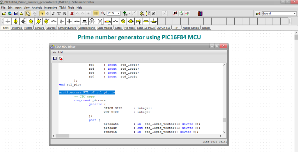
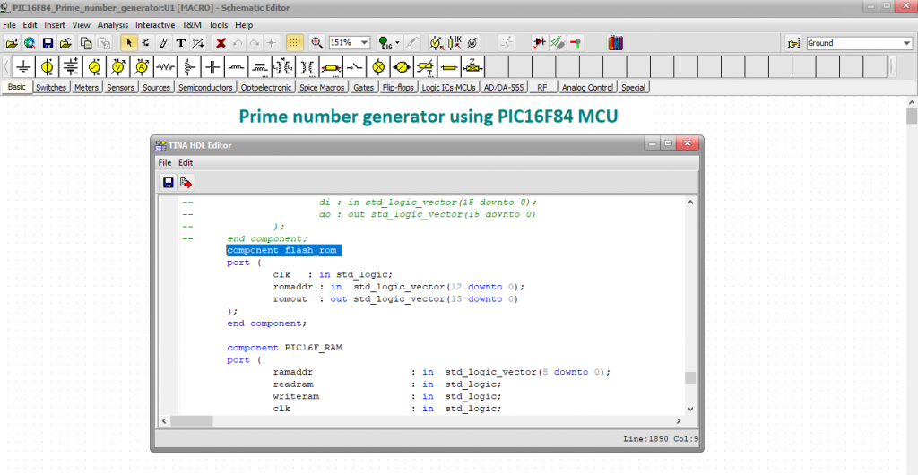
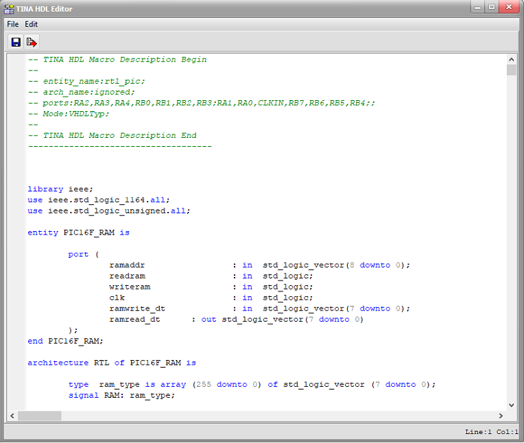
The PIC MCU model is written in VHDL.
The VHDL code is the functional model of a PIC16F84 8-bit microcontroller with initialized flash program memory.
CLK1 provides the external 10-MHz clock.
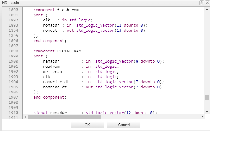
Looking at the VHDL code
Next, we look at the VHDL code using TINA HDL Editor.
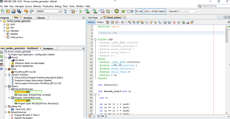
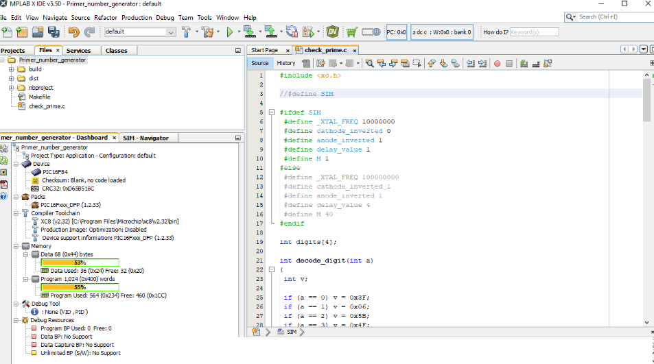
Checking the C code
In the following, we will check the program code written in C and converted to this VHDL code.
The project was created, and the program was developed with the free version of Microchip MPLAB IDE and their Microchip XC8 compiler.
We start MBLAB.
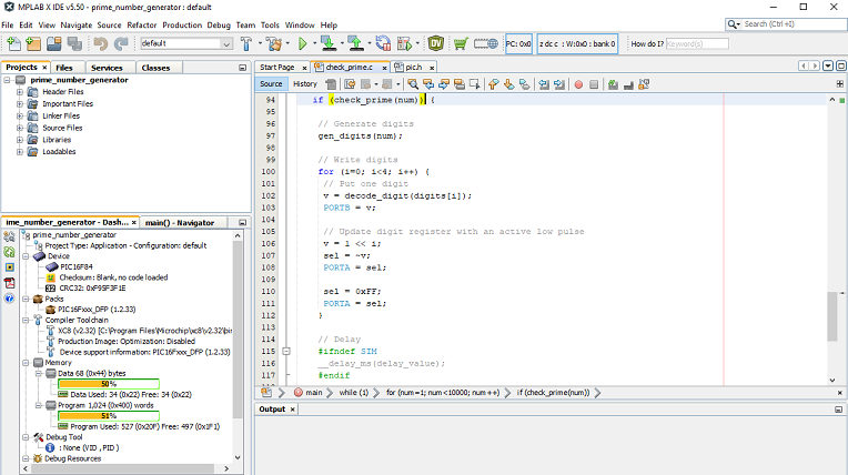
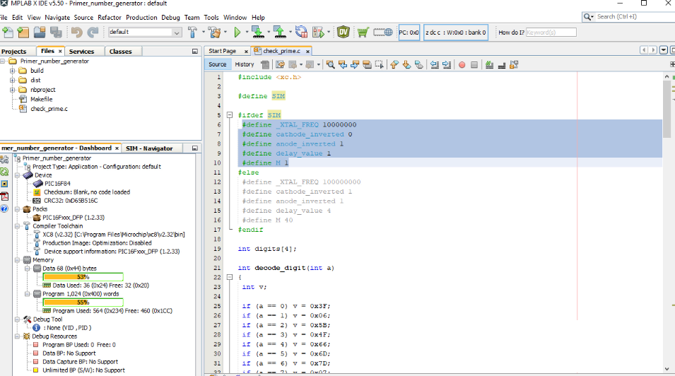
First, we define SIM, indicating that we are running a simulation.
The code writes prime numbers between 1 and 9999 with the help of a for loop starting from line 77.
A digit is displayed by writing the representative 7-segment code to the digit’s external register.
Digital circuit simulation
After that, we return to TINA’s Schematic Editor to test our circuit with digital circuit simulation.
Testing our circuit in a real environment
Making the main difference in the C code for the Synthesis
Then, we’ll open again the MPLAB editor to make the main difference in the C code for the synthesis, like the processor speed (50 MHz). This is the oscillator frequency of the Terasic DE10-Lite FPGA board.
Compiling the project
Next, we compile the project and convert the result – the executable binary – into VHDL. The code is placed in the flash ROM component of our VHDL PIC model.
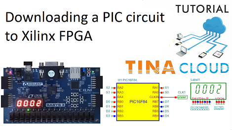
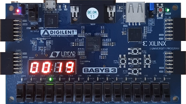
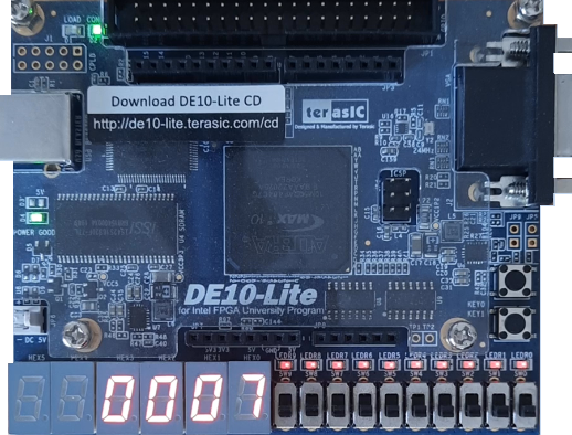
PIC16F84 Prime number generator DE10 Lite circuit
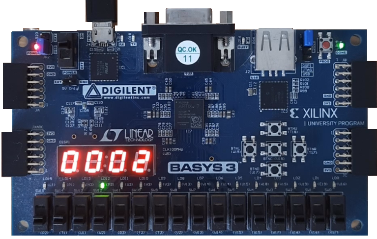
Finally, we will test our circuit, ” PIC16F84 Prime number generator DE10 Lite ” in a real environment using the Terasic DE10-Lite FPGA board.
We have FPGA pins connected to the segments of the displays and the clock input pin of the PIC MCU.
The com pin of the displays can be left floating as the common anode of the digits is hardwired on the board.
Using the Quartus Prime Lite software to program the hardware
We will export the VHDL to the Quartus Prime Lite software, compile it and load the resulting bitstream into the Terasic DE10-Lite FPGA development board.
Testing the circuit with the Terasic DE10-Lite board
As soon as we finish programming the hardware and we turn the Terasic DE10-Lite board on, we can see the prime numbers written on the display as expected.
Watch our video to learn more.
You can learn more about TINA here: www.tina.com
You can learn more about TINACloud here: www.tinacloud.com