The Half Adder is a so called combinational circuit, to add two single binary digits and provide the output plus a carry value. It has two inputs, called A and B, and two outputs S (Sum) and C (Carry).
The relation between inputs (A, B) and the outputs (Sum. Carry) is described by the so called Truth Table. The Truth Table for the Half Adder is as follows:
In this tutorial video we created and tested a Half Adder circuit using TINACloud.
We used basic OR, AND, NOT (Inverter) gates, High-Low switches and Voltage pins for the outputs.
Click here to watch our tutorial video and learn more.
The Half Adder is a so called combinational circuit, to add two single binary digits and provide the output plus a carry value. It has two inputs, called A and B, and two outputs S (Sum) and C (Carry).
The relation between inputs (A, B) and the outputs (Sum. Carry) is described by the so called Truth Table. The Truth Table for the Half Adder is as follows:
In this tutorial video we created and tested a Half Adder circuit using TINA.
We used basic OR, AND, NOT (Inverter) gates, High-Low switches and Voltage pins for the outputs.
Click here to watch our tutorial video and learn more.
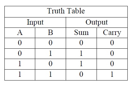
The half adder is a simple combinational circuit, to add two single binary digits and provide the output plus a carry value. It has two inputs, called A and B, and two outputs S (Sum) and C (Carry).
The relation between inputs (A, B) and the outputs (Sum. Carry) is described by the so called Truth Table. The Truth Table for the Half Adder is as follows:
In this tutorial video we will create and test a Hal Adder circuit in TINA.
To start with, we will draw the schematic diagram of the half adder. We will use an XOR gate for the Sum and an AND gate for the Carry, High-Low switches and Voltage pins for the outputs. We will then test the circuit operation using Transient analysis and the Interactive mode of TINA.
Click here to watch our tutorial video and learn more.
TINA includes a very powerful mixed mode circuit simulator engine. It is based on the XSPICE mixed mode algorithm, extended with MCU and HDL (VHDL, Verilog, Verilog A & AMS) components. In your circuits you may freely mix any analog or digital components of TINA, including microcontrollers (MCUs) and macros with Spice or HDL content. You can modify these components on the fly along with the code in the MCUs. TINA will analyze the analog parts in analog, the digital parts in digital, and will automatically create the interfaces among the components. This ensures synchronization and fast convergence.
Let’s explore some of the uses of this mode through a few examples.
1. Waveform generation with VHDL and Spice subcircuits
The following circuit generates an analog sine or sawtooth signal depending on the status of the left SW-MODE switch:
Click the picture to run this circuit online with TINACloud
The Digital Wave box on the left of the circuit includes VHDL code with a lookup table (Sine_LUT ) for the sine wave and a counter for the sawtooth signal. The essential part of the VHDL code is:
   process(Reset, Clk)
   begin
       if (Reset = '1') then
           Wave <= (others => '0');
           LUT_index <= 0;
       elsif rising_edge(Clk) then
           if (Enable = '0') then
               Wave <= (others => '0');
           elsif (Sel = '0') then
               Wave <= Sine_LUT(LUT_index);
           else
               Wave <= conv_std_logic_vector(LUT_index,5);
           end if;
           if (LUT_index = LUT_index_max) then
               LUT_index <= 0;
           else
               LUT_index <= LUT_index + 1;
           end if;
       end if;
   end process;
   d0 <= Wave(0); d1 <= Wave(1); d2 <= Wave(2); d3 <= Wave(3); d4 <= Wave(4);
The digital output of the counter is converted into an analog signal in the 5 bit DA converter of TINA shown in the middle of the circuit. The DAC sine wave output needs to be cleaned up with a low pass filter. We will use a Spice opamp model of the TL081 in a Sallen and Key low pass filter configuration. Press the Enter Macro button on the property dialog and TINA will open the macro. You can review and, if necessary, modify the Spice code inside the macro.
Here are the final waveforms of the full circuit, including the five counter output waveforms. SW_MODE is in the High state, selecting the sawtooth signal:
If we change the SW-MODE switch to Low and run Transient analysis again, the waveforms are:
To see the effect of the analog filter, delete curves d0 to d4 from the diagram by clicking the curves and pressing the Del key:
2. MCU controlled SMPS circuit
The mixed mode simulator of TINA not only allows MCUs, but also any linear or nonlinear parts in TINA’s libraries. As an example, let’s study the following circuit, which realizes a DC-DC converter, converting 5V DC to 13V DC, and operating in boost mode:
Boost Converter with PIC control
Click the picture to run this circuit online with TINACloud
The waveforms below demonstrate how the analog parts and the MCU interact in TINA.
3. Mixed circuit example consisting of simple analog and digital components
PSK demodulator
Click the picture to run this circuit online with TINACloud
You can display the results in one diagram or as separate diagrams shown below by simply appending a colon ( : ) and a number to each output name.
Mixed mode results:
Download the FREE trial demo of TINA Design Suite and get:
One year free access to TINACloud (the cloud-based, multi-language, installation-free online version of TINA now running in your browser anywhere in the world.)
An immediate 20% discount from the offline version of TINA
Free license for your second computer, laptop etc.
Click here to download the FREE trial demo of TINA
Adding a capacitor in parallel with the feedback resistor of an op amp is an easy way of accomplishing low- pass filtering. This technique works quite well in an inverting amplifier (see the curves below) but not necessarily in a non-inverting amplifier. If the NI amplifier has high gain, the filtering is not bad– but inferior to the inverting case. As the NI amplifier gain is reduced, the filter effectiveness suffers. In a gain of +2V/V, there is only 6dB of stopband attenuation. In a voltage-follower (gain of +1V/V), there is no low- pass filtering at all! In each amplifier, the value of R2 was stepped logarithmically from 100 ohms to 100k.\e(x,2) (Circuit is created by Neil P. Albaugh, TI-Tucson )
Circuit for Demonstration of Pitfalls related with the Feedback Capacitor in Low-pass Filters
Feedback Capacitor Low-Pass Filter Pitfalls
Demonstration of Pitfalls related with the Feedback Capacitor in Low-pass Filters circuits
The great feature of the TINA circuit simulator that you can analyze this circuit immediately with TINACloud the online version of TINA.
You can send this link to any TINACloud customers and they can immediately load it by a single click and then run using TINACloud.
Download the FREE trial demo of TINA Design Suite and get
One year free access to TINACloud (the cloud-based, multi-language, installation-free online version of TINA now running in your browser anywhere in the world.)
An immediate 20% discount from the offline version of TINA
Free license for your second computer, laptop etc.
Click here to download the FREE trial demo of TINA