to see how to create a TINA macro component using a THS4121 Spice Subcircuit downloaded previously from the web.
Download the FREE trial demo of TINA Design Suite and get:
One year free access to TINACloud (the cloud-based, multi-language, installation-free online version of TINA now running in your browser anywhere in the world.)
An immediate 20% discount from the offline version of TINA
Free license for your second computer, laptop etc.
Click here to download the FREE trial demo of TINA
to see how to create an UA741 Operational Amplifier model using a Spice Subcircuit in TINA:
Download the FREE trial demo of TINA Design Suite and get:
One year free access to TINACloud (the cloud-based, multi-language, installation-free online version of TINA now running in your browser anywhere in the world.)
An immediate 20% discount from the offline version of TINA
Free license for your second computer, laptop etc.
Click here to download the FREE trial demo of TINA
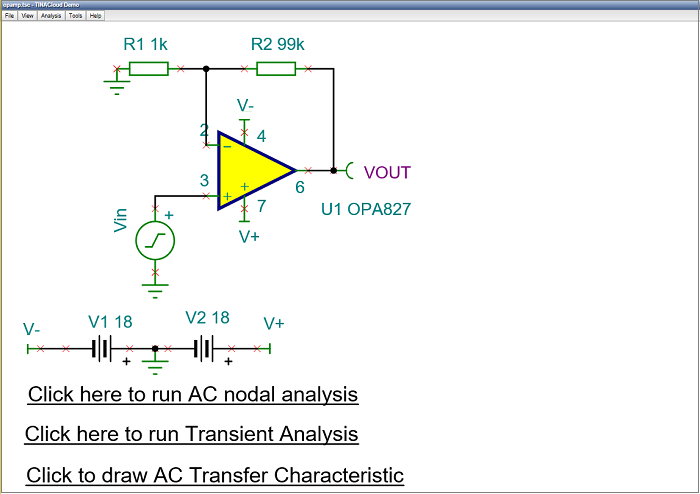
A new exciting feature in TINACloud that now you can add links to your circuits
which allow you to carry our most TINACloud analyses simply by clicking the links without using TINAclouds’s menus. This feature is extremely useful when you create presentations for your customers.
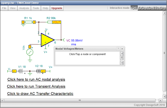
For example if you click the “Click here to run AC nodal analysis” link the following screen will appear.
By default is shows the rms voltage on the output(s). If you click with the cursor on any nodes (yellow boxes) of the circuit it will display the detailed nodal analysis data in a small window. Click You can repeat this any times until you press the Close button to finish the Nodal Analysis.
Further if you click the “Click here to run AC transient analysis” link, the Transient analysis will automatically run and the following screen will appear. You can now run cursor on the diagram or close the diagram and make further analyses.
Download the FREE trial demo of TINA Design Suite and get:
One year free access to TINACloud (the cloud-based, multi-language, installation-free online version of TINA now running in your browser anywhere in the world.)
An immediate 20% discount from the offline version of TINA
Free license for your second computer, laptop etc.
TINA includes a very powerful mixed mode circuit simulator engine. It is based on the XSPICE mixed mode algorithm, extended with MCU and HDL (VHDL, Verilog, Verilog A & AMS) components. In your circuits you may freely mix any analog or digital components of TINA, including microcontrollers (MCUs) and macros with Spice or HDL content. You can modify these components on the fly along with the code in the MCUs. TINA will analyze the analog parts in analog, the digital parts in digital, and will automatically create the interfaces among the components. This ensures synchronization and fast convergence.
Let’s explore some of the uses of this mode through a few examples.
1. Waveform generation with VHDL and Spice subcircuits
The following circuit generates an analog sine or sawtooth signal depending on the status of the left SW-MODE switch:
Click the picture to run this circuit online with TINACloud
The Digital Wave box on the left of the circuit includes VHDL code with a lookup table (Sine_LUT ) for the sine wave and a counter for the sawtooth signal. The essential part of the VHDL code is:
   process(Reset, Clk)
   begin
       if (Reset = '1') then
           Wave <= (others => '0');
           LUT_index <= 0;
       elsif rising_edge(Clk) then
           if (Enable = '0') then
               Wave <= (others => '0');
           elsif (Sel = '0') then
               Wave <= Sine_LUT(LUT_index);
           else
               Wave <= conv_std_logic_vector(LUT_index,5);
           end if;
           if (LUT_index = LUT_index_max) then
               LUT_index <= 0;
           else
               LUT_index <= LUT_index + 1;
           end if;
       end if;
   end process;
   d0 <= Wave(0); d1 <= Wave(1); d2 <= Wave(2); d3 <= Wave(3); d4 <= Wave(4);
The digital output of the counter is converted into an analog signal in the 5 bit DA converter of TINA shown in the middle of the circuit. The DAC sine wave output needs to be cleaned up with a low pass filter. We will use a Spice opamp model of the TL081 in a Sallen and Key low pass filter configuration. Press the Enter Macro button on the property dialog and TINA will open the macro. You can review and, if necessary, modify the Spice code inside the macro.
Here are the final waveforms of the full circuit, including the five counter output waveforms. SW_MODE is in the High state, selecting the sawtooth signal:
If we change the SW-MODE switch to Low and run Transient analysis again, the waveforms are:
To see the effect of the analog filter, delete curves d0 to d4 from the diagram by clicking the curves and pressing the Del key:
2. MCU controlled SMPS circuit
The mixed mode simulator of TINA not only allows MCUs, but also any linear or nonlinear parts in TINA’s libraries. As an example, let’s study the following circuit, which realizes a DC-DC converter, converting 5V DC to 13V DC, and operating in boost mode:
Boost Converter with PIC control
Click the picture to run this circuit online with TINACloud
The waveforms below demonstrate how the analog parts and the MCU interact in TINA.
3. Mixed circuit example consisting of simple analog and digital components
PSK demodulator
Click the picture to run this circuit online with TINACloud
You can display the results in one diagram or as separate diagrams shown below by simply appending a colon ( : ) and a number to each output name.
Mixed mode results:
Download the FREE trial demo of TINA Design Suite and get:
One year free access to TINACloud (the cloud-based, multi-language, installation-free online version of TINA now running in your browser anywhere in the world.)
An immediate 20% discount from the offline version of TINA
Free license for your second computer, laptop etc.
Click here to download the FREE trial demo of TINA
TINA Design Suite is a powerful yet affordable circuit simulator and PCB design software package for analyzing, designing, and real time testing of analog, digital, HDL, MCU, and mixed electronic circuits and their PCB layouts.
You can also analyze SMPS, RF, communication, and optoelectronic circuits; generate and debug MCU code using the integrated flowchart tool; and test microcontroller applications in a mixed circuit environment.
A great number of electrical engineers find TINA an easy to use, high performance tool, while educators welcome its unique features for the training environment. TINA also includes a unique feature, Symbolic Analysis.
Symbolic analysis produces
the closed form expression of the transfer function, equivalent resistance, impedance, or response of analog linear networks. In DC and AC analysis mode, TINA derives formulas in full-symbolic or semi-symbolic form. In transient analysis, the response is determined as a function of time. Circuit variables can be referenced either as symbolic names or by value on a component-by-component basis. Through symbolic analysis, poles and zeros of linear circuits can be calculated and plotted. You can efficiently prepare reports and paper presentations by printing or by copying and pasting your expressions to any Windows program.
Watch ourtutorial video to see how to use the Symbolic Analysis of Analog Circuits in TINA.
Download the FREE trial demo of TINA Design Suite and get:
One year free access to TINACloud (the cloud-based, multi-language, installation-free online version of TINA now running in your browser anywhere in the world.)
An immediate 20% discount from the offline version of TINA
Free license for your second computer, laptop etc.