Cload Compensation
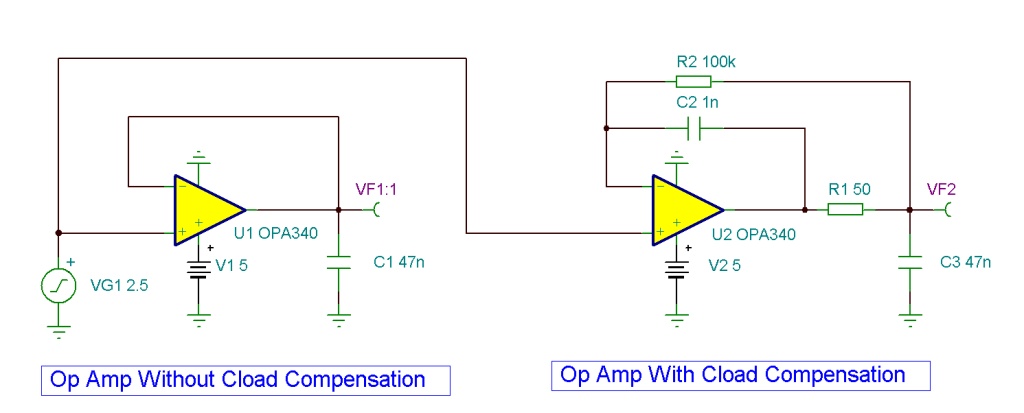
Driving a capacitive load directly with an op amp is an invitation to instability or oscillation. The amplifier’s output resistance and the load capacitance form a pole in the feedback circuit. This inserts additional phase shift which will reduce the loop phase margin– perhaps to zero.
The effects of reduced phase margin can be seen in the waveform ringing and gain peaking plots below. By isolating the capacitance with a small resistor (R1) and providing local high-frequency feedback (C2), very little phase margin is lost. The voltage drop across R1 is sensed by a DC feedback connection (R2) to the circuit output and thereby reduced to virtually zero.
Note the improvement gained by compensating for a Cload! (Circuit is created by Neil P. Albaugh, TI – Tucson)

Online Simulation of the Cload Compensation Circuit
The great feature of the TINA circuit simulator that you can analyze this circuit immediately with TINACloud the online version of TINA. Of course you can also run this circuit in the off-line version of TINA.
Click here to invoke TINACloud and analyze the circuit.
You can send this link to any TINACloud customers and they can immediatelly load it by a single click and then run using TINACloud.
Michael Koltai
www.tina.com
