Migrating your circuit designs between different electronic design automation (EDA) tools can often be a challenge, but it doesn’t have to be. In this guide, you will learn how to seamlessly convert both offline Multisim and Multisim Live circuits to run directly in the offline version of TINA.
Whether your files are saved in the classic desktop formats (.ms13 or .ms14) or as cloud-based .msjs files from Multisim Live, TINA handles them smoothly. Furthermore, because the converted .tsc files are completely cross-compatible, you can easily jump between offline TINA and TINACloud without missing a beat.
Click here or on the image above to watch this blog presented as a video tutorial.
Let’s walk through four practical examples to see this conversion tool in action, spanning analog, digital, RF, and power management circuits.
Example 1: FM Demodulation Circuit
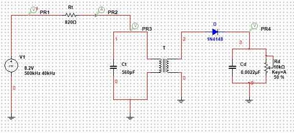
To demonstrate how the conversion works, we will start with an FM Slope Detector circuit. Because this design is available in both formats, we will begin by importing the Multisim Live version first.
- Start TINA and go to the File menu.
- Select Import > Multisim file.
- Choose the FM Slope Detector.msjs file. The converted circuit will instantly appear right inside the TINA schematic editor.
Alternatively, you can follow the exact same steps to import the offline Multisim (.ms14) version. The same clean schematic diagram will appear.
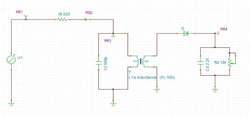
FM Demodulation Circuit in TINA
This specific design is configured to process a frequency-modulated signal featuring a 500 kHz carrier and a 40 kHz modulating frequency.
Parameter Check and Waveform Organization
Before running a simulation, it is always a good practice to verify your signal parameters:
- Double-click the Voltage Generator, then click the Details (…) button in the Signal field.
- The FM Signal parameters will appear alongside a helpful preview of the waveform to ensure the carrier and modulating frequencies are correct.
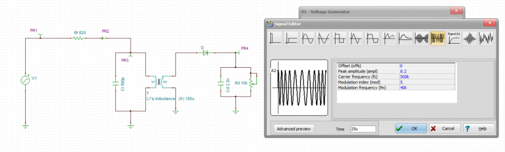
FM Demodulation Circuit: Parameter Check
To optimize the final output display, we can modify the PR4 output label. By changing the label to PR4:1, TINA will automatically separate the curves during analysis and position the PR4 trace at the very top of the diagram.
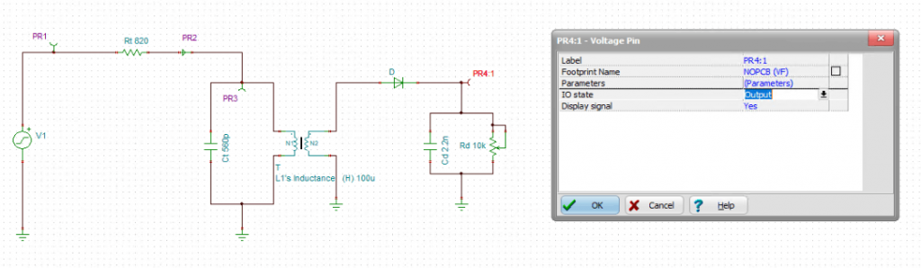
FM Demodulation Circuit: Waveform Organization
Transient Analysis and Verification
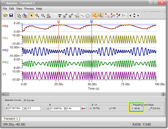
Navigate to the analysis menu and run a Transient Analysis. Once the results are displayed, zoom in on a few periods of the modulating signal to get a clear, detailed view of both the FM signal and the demodulated output.
To verify the results mathematically, place two cursors on the PR4 output waveform. Measuring the time difference between neighboring peaks allows you to determine the signal period. This confirms that the output frequency is indeed 40 kHz, matching the original modulating signal perfectly.
Example 2: Half Adder Digital Circuit
Our second example is a digital circuit in the Multisim Live (.msjs) format. This feature is especially valuable because Multisim Live does not currently support the conversion of digital circuits to the offline MS14 format, which limits their use in a standard desktop Multisim environment. TINA bridges this gap perfectly.
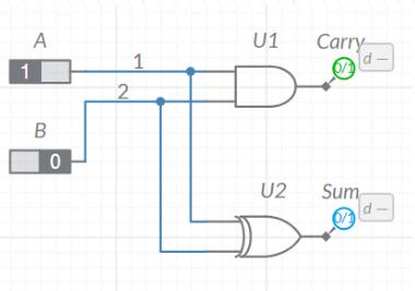
Half Adder circuit in Multisim
To begin, use the Import command to open your .msjs digital file in TINA.
Testing the Digital Circuit
Once the circuit appears on your screen, you can begin live testing. A standout feature of TINA is its ability to display active digital states in real-time—not just on the final outputs, but across every visible digital node on the schematic.
- Press the Dig (Interactive Digital) button to start the interactive simulation.
- Change Switch A to High; you will immediately see the state change to logic high at the Sum output.
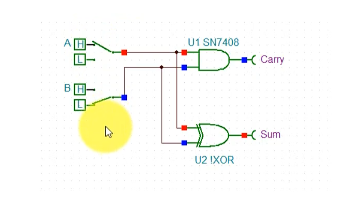
Half Adder circuit in TINA: Changing Switch A to high
- Set the input switches so only Switch B is High, and the Sum remains high.
- Turn both the A and B switches ON (both inputs High). The Sum drops to Low and the Carry becomes High.
This interactive test successfully confirms the standard logic operation of a Half Adder.
VHDL and Verilog Subcircuits
Digital design in modern electronics rarely relies purely on individual logic gates; instead, designers use Hardware Description Languages (HDLs) like VHDL and Verilog. These descriptions can be synthesized directly into integrated circuits like FPGAs.
TINA and TINACloud support this advanced workflow by allowing you to embed HDL macros directly into your schematics as subcircuits.
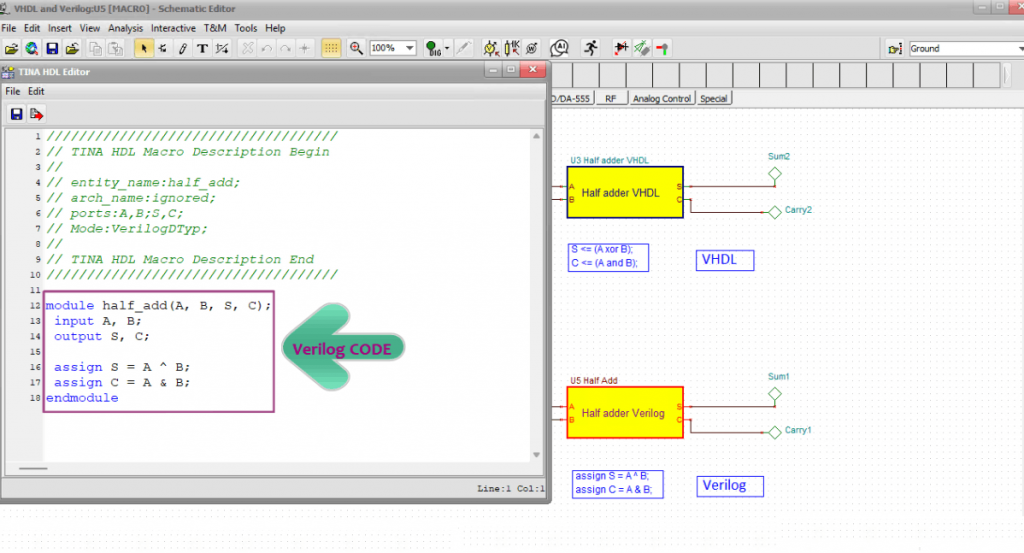
To view the underlying code of an HDL subcircuit:
- Double-click the Half Adder VHDL macro block.
- Click the Enter Macro button in the dialog box.
- An HDL code window will appear, displaying the exact VHDL syntax.
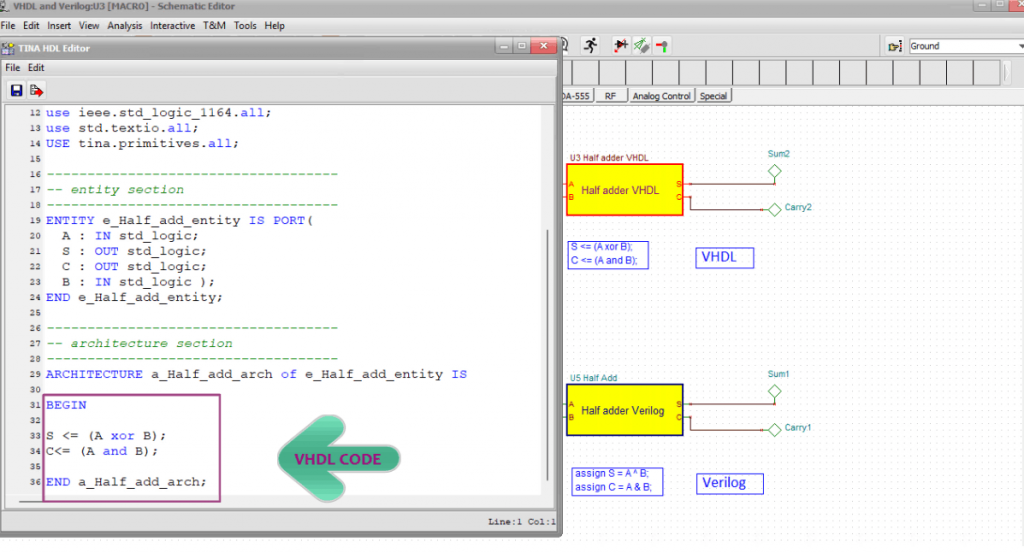
You can follow the exact same steps to view the equations inside a Verilog macro.
Comparing Gate Logic vs. HDL
Close the macro windows and press the Interactive Digital button once again to test the entire system simultaneously.
Whether you toggle a single input high or turn both inputs high, you will observe that the traditional logic gates, the VHDL macro, and the Verilog macro produce identical output states. Using HDLs allows designers to work at a much higher level of abstraction, making complex digital development faster and more efficient.
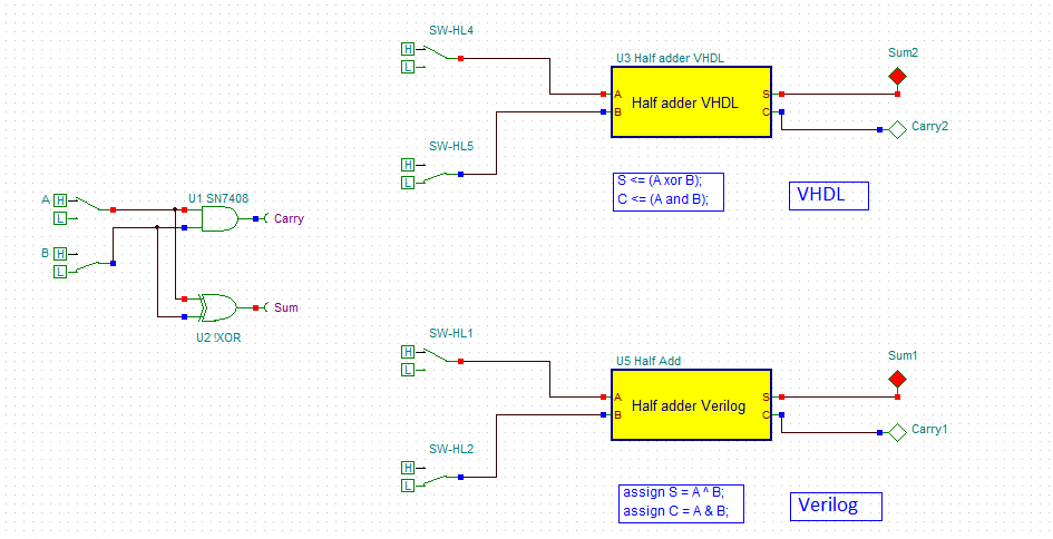
Half Adder with VHDL and Verilog subcircuits: Interactive Digital Simulation
For more information on creating and uploading digital circuits to Xilinx and Intel FPGA boards using VHDL, Verilog, or schematic designs, visit our YouTube channel: https://www.youtube.com/@TinaDesignSuite

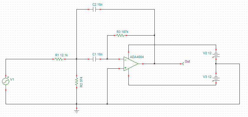
Example 3: Active Bandpass Filter
For our third example, save your Multisim (.ms14 or .msjs) active filter file to your hard drive, then import it into TINA. The schematic will open automatically in the circuit editor, where you can save it locally as a standard TINA .tsc file.
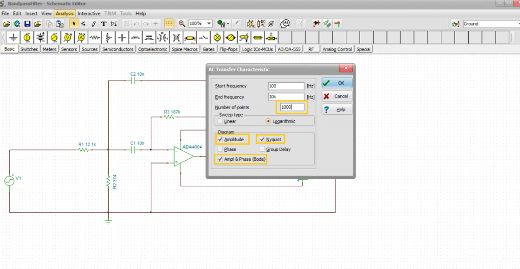
Configure and Run the AC Analysis
Go to the Analysis menu and select AC Analysis > AC Transfer Characteristic… In addition to standard AC Bode plots, TINA can calculate Amplitude, Phase, Nyquist, and Group Delay diagrams. For this simulation, select the AC Bode, Amplitude, and Nyquist diagrams. Set the number of points to 1000 for high-resolution curves, and click OK. Three separate tabs will appear displaying your results.
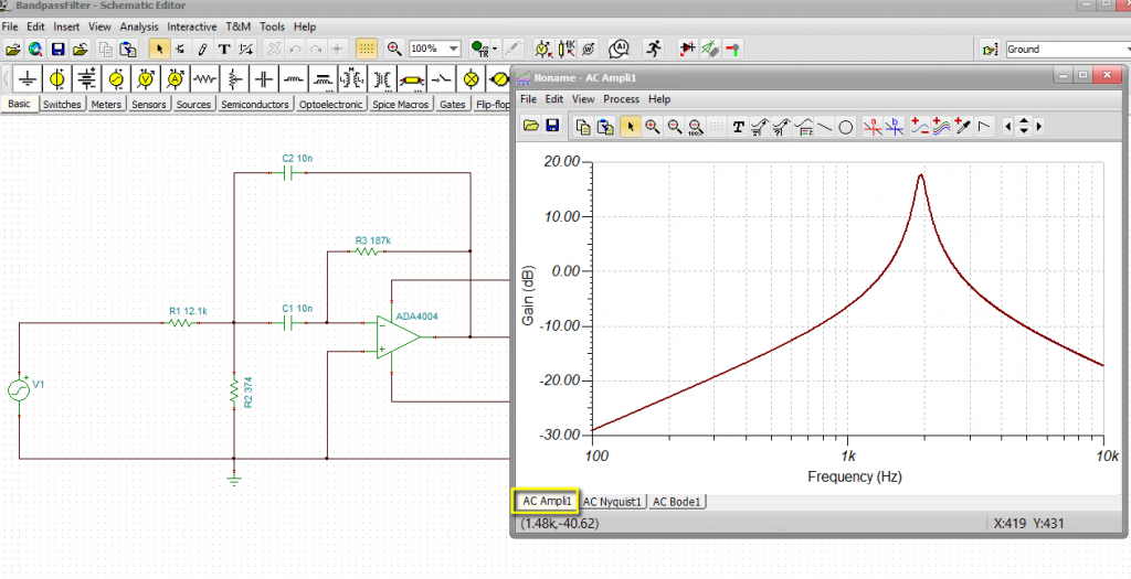
Active Bandpass Filter circuit: AC Amplitude diagram
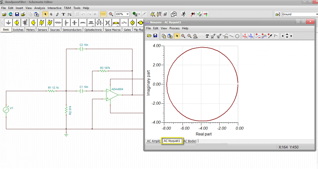
Active Bandpass Filter circuit: AC Nyquist diagram
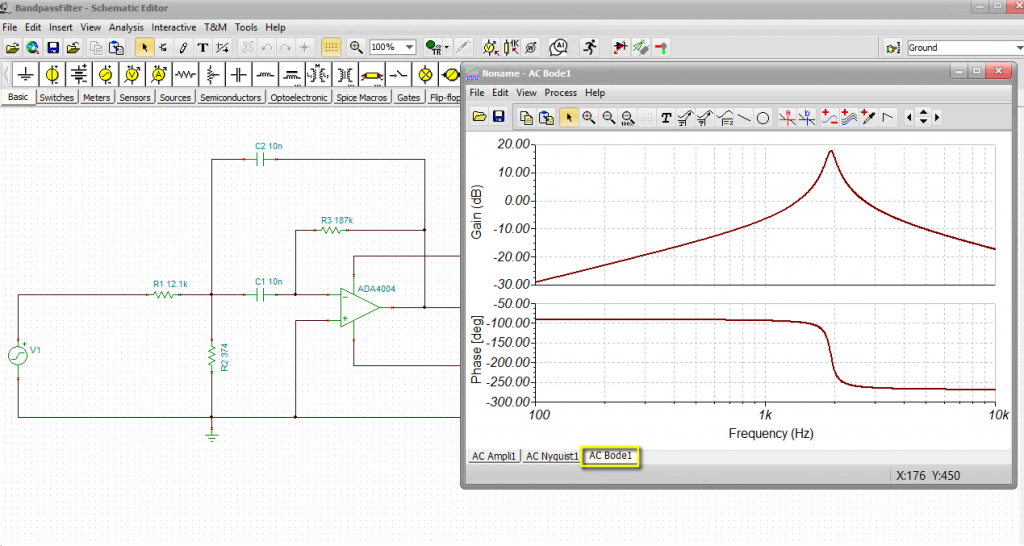
Active Bandpass Filter circuit: AC Bode diagram
Symbolic Analysis in TINA
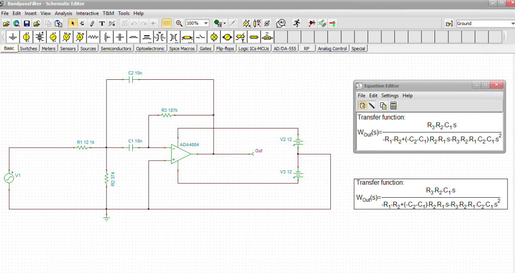
A truly unique feature of TINA and TINACloud is the ability to derive a circuit’s Transfer Function symbolically, presenting it as an exact mathematical formula rather than just a plotted curve. This provides engineers and students with deeper insights into exact circuit behavior—including poles, zeros, gain, and frequency response.
Note: While symbolic transfer function derivation is only possible for linear circuits, you can still easily analyze active filters. By replacing complex, nonlinear operational amplifier models with ideal op-amps, TINA can derive highly accurate symbolic transfer functions.
To run this:
- Go to the Analysis menu.
- Select Symbolic Analysis > AC Transfer.
- The analytical form of the Transfer Function will immediately display in the Equation Editor.
Documenting the Schematic
To add this formula directly to your technical documentation, click the Copy icon inside the Equation Editor window. Switch back to the TINA Schematic Editor, select Edit > Paste, and left-click to place the mathematical formula directly onto your schematic canvas.
Plotting and Comparing Results
You can also plot this analytical formula to verify it against your numerical simulation:
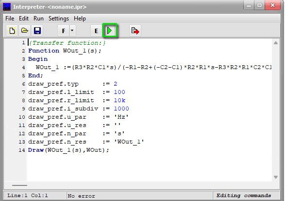
- In the Equation Editor, click the Interpreter calculator icon.
- Inside the Interpreter window, press the green arrow to run the calculation.
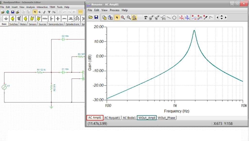
- Once the transfer function plot appears, change its curve color to green and click the Copy curve icon.
- Switch back to your original, numerically calculated Ampl 1 tab and click Paste Curve.
As you will see, the analytical and numerical curves match perfectly. This confirms that using ideal operational amplifiers in filter synthesis yields highly accurate results.
Example 4: Inverting DC-DC Converter
Our final example is a power electronics circuit: an inverting DC-DC converter based on the MC34063 switching regulator from onsemi. This circuit efficiently converts a +5 V input down to a −12 V output.
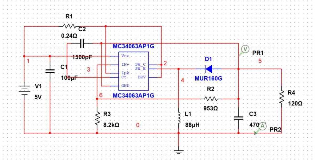
Once converted from its original Multisim format, you will find that these switching circuits run at identical or even faster simulation speeds within TINA. Simply save your .ms14 or .msjs file, select File > Import, and open it in TINA.
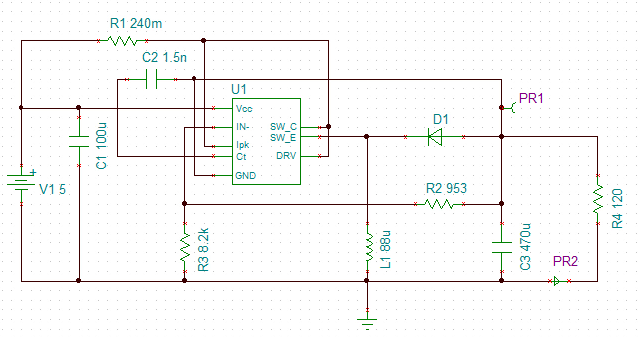
Inverting DC-DC Converter circuit in TINA
Running the Analysis and Customizing the Display
Navigate to the analysis menu, select Transient Analysis, and run the simulation.
To get a clean, detailed view of the switching waveforms, we can customize the diagram layout:
- Click the View tab in the diagram window and select Separate curves.
- Click on the PR1 axis to manually adjust its display limits to fit the waveform perfectly, and repeat the procedure for the PR2 axis.
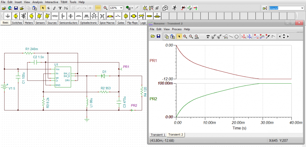
Inverting DC-DC Converter circuit: Running Transient Analysis & Customizing the Display
Component Library Tip:
If you are building power designs from scratch, note that TINA and TINACloud include a massive library of built-in DC-DC converter ICs and evaluation circuits from leading manufacturers, including Texas Instruments, Infineon, Analog Devices, Nisshinbo Micro Devices, Würth Elektronik, STMicroelectronics, and Semtech.
Conclusion
Migrating your designs from desktop Multisim or Multisim Live to TINA is quick, seamless, and preserves the integrity of your analog, digital, and power schematics. By combining TINA’s powerful interactive modes, symbolic analysis capabilities, and fast simulation engines, you can take your circuit verification to the next level.
- 📺 Watch the complete video tutorial: Watch on YouTube
- 🌐 Explore the software & features: Visit TINA Official Website