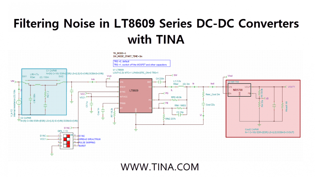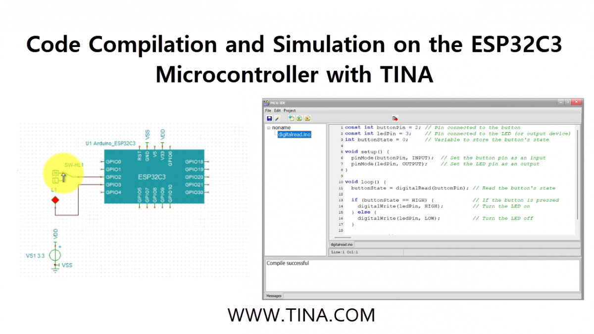
Our latest video guide is now available, featuring a comprehensive walkthrough of Code Compilation and Simulation on the ESP32C3 Microcontroller using TINA v16.
Prerequisites
Before you begin, ensure your environment is correctly configured:
- Compiler Installation: During the TINA installation process, you must have selected the ESP32 compiler package.
- Note: If you missed this, you can add it later by running a Custom installation and enabling the ESP32 Compiler checkbox.
- Arduino Path Setup: Navigate to
Analysis>Options>Digital Simulation>Advanced. Ensure the Arduino path is correctly set to your local installation.
Step 1: Creating a New Project
- Open TINA and locate the Logic_ICs-MCUs tab on the toolbar.
- Click the Arduino button.
- From the dropdown list, select the ESP32C3 microcontroller and place it onto your schematic workspace.
Step 2: Compiling Arduino Code
Open the Editor: Right-click on the ESP32C3 component and select Open MCU code editor…
Add Your Code: In the code editor window, click the “Add Existing file to Project” button to load your previously saved Arduino (.ino) program.
Compile: Press the “Make Project” button on the toolbar. TINA will now compile your code using the integrated ESP32 compiler.
Save: Once the compilation is successful, press the “Save Project” button and close the editor window.
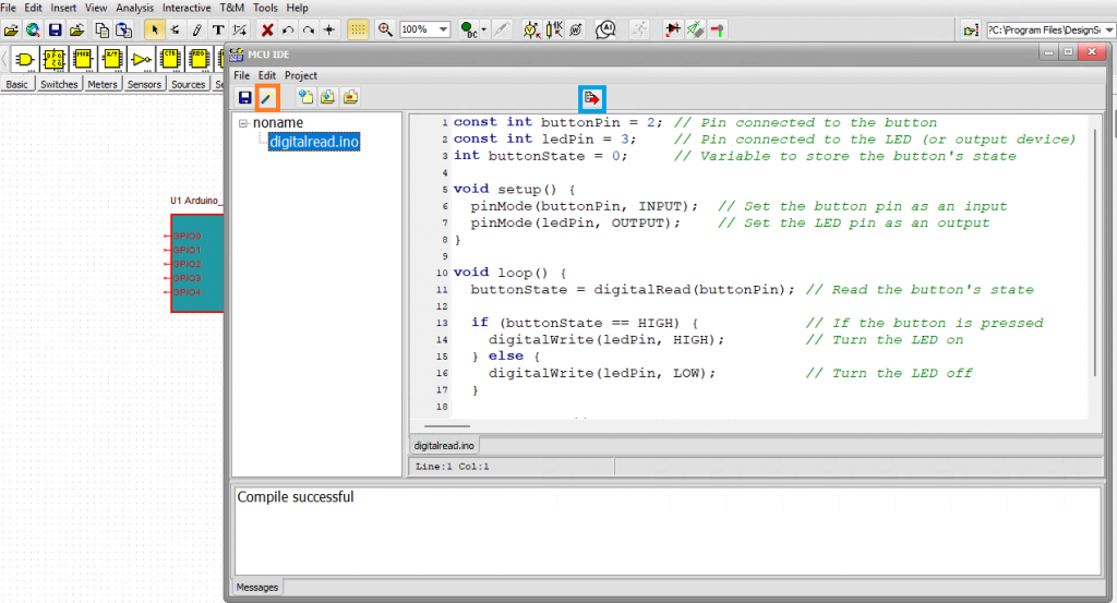
ESP32C3 Microcontroller: Compiling and saving the Arduino code
Step 3: Building the Circuit
- Add Components: Connect a switch to a GPIO input and an LED to a GPIO output.
- Ready-to-Use Example: If you want to see a completed version of this setup, you can find it in the built-in examples:
TINA Examples/Microcontrollers/ESP32/esp32c3_digitalread.tsc
Step 4: Running the Simulation
This example is designed to read the state of a physical switch. Depending on the switch position, the ESP32C3 will turn the LED on or off.
- Press the TR (Interactive Transient) button to start the simulation.
- Toggle the switch: Watch as the LED responds instantly to the input change.
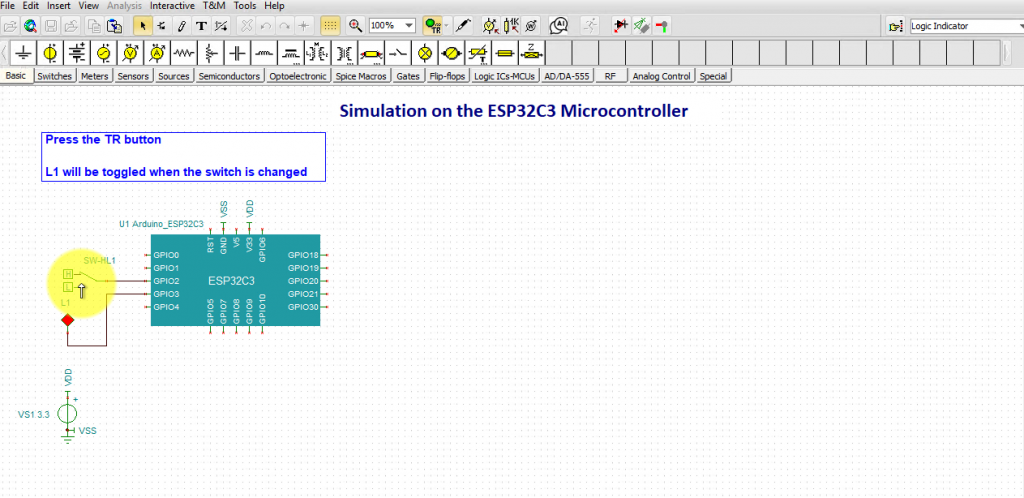
ESP32C3 Microcontroller: Toggling the switch
Conclusion
By following these steps, you can rapidly prototype and debug your ESP32C3 applications in a risk-free virtual environment. TINA v16’s ability to compile Arduino code directly and simulate it alongside analog components makes it an invaluable tool for modern embedded design.