
2. Level Shifters
 CURRENT – 2. Level Shifters
 PREVIOUS- 1. Differential amplifiers
Level Shifters
Even if the input to an amplifier has an average value of zero volts, the output often has a non-zero average voltage due to biasing effects. These dc voltages can cause an undesired offset which adversely affects the operation of a system.
Since the op-amp is a multi-stage dc amplifier with high gain, unwanted dc voltages can be a source of concern. A small offset in an early stage can saturate a later stage.
Level shifters are amplifiers that add or subtract a known voltage from the input in order to compensate for dc offset voltages. Op-amps have level shifters included in their design.
Figure 7 illustrates a simple level shifter. We show that this shifter acts as a unit-gain amplifier for ac while providing an adjustable dc output.
We begin the analysis by using KVL in the input loop of Figure 7(a) and letting vin = 0 to obtain
(34)
Now since
(35)
we solve for the dc value of output voltage, Vout.
(36)
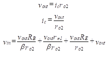
Equation (36) shows that by varying RE, Vout can be set to any desired dc level (limited to a maximum of VBB–VBE). Since VBB is the dc level acquired from the previous stage, this amplifier is used to shift the level downward (to a lower value). If upward shifting is required, a similar circuit is used but pnp transistors are substituted for the npn transistors. A complete circuit with active current source is shown in Figure 7(b).
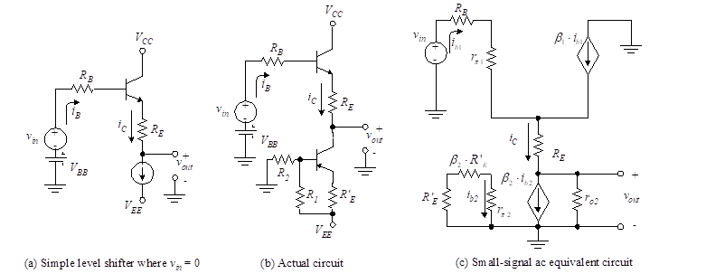
Figure 7– Level shifter
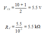
We now examine the circuit with ac signals applied. Figure 7(c) illustrates the ac equivalent circuit. Note that β2ib2 is the collector current in the active current source, and we assume it to be a constant. Because the ac value of the current is zero, this current source is replaced by an open circuit. We write the ac equations using KVL.
(37)
and
(38)
The ratio of ac output to ac input is
(39)
Equation (39) shows that as ro2 becomes large, the ratio of output to input approaches unity and the level shifter acts like an emitter follower to ac. This is the desired result.
Example
Two direct-coupled CE amplifiers are placed in series to achieve the desired voltage gain. Design a level shifter to be placed in between the two CE amplifiers to provide a dc voltage sufficiently low to prevent the second CE amplifier from saturating. Do this by providing a 1 V bias to the second stage. The collector voltage, VC, of the first amplifier is 4 V, and the RC of that amplifier is 1 kΩ. Design the level shifter to have an IC of 1 mA using a ![]() power supply. Use a current source of the type shown in Figure 3 (See chapter: Differential amplifier 1.3) with transistors having β(s) = 100, VBE(s) = 0.7 V, and VON = 0.7 V.
power supply. Use a current source of the type shown in Figure 3 (See chapter: Differential amplifier 1.3) with transistors having β(s) = 100, VBE(s) = 0.7 V, and VON = 0.7 V.
Solution: The level shifter is shown in Figure 7(b). We need to find the values of RE, R1, R2, and R’E. Since the first amplifier has a VC of 4 V, the value of VBB for Equation (36) is 4 V, whereas the RB of that formula is 1 kΩ. Note this is using the Thevenin equivalent circuit of the previous amplifier. Equation (36) then yields,
![]()
Setting the current-source transistor operating point in the middle of the dc load line, we have
![]()
and
The voltage across R’E is 5.5 V. Then
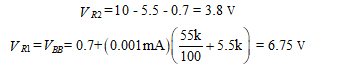
We now know the voltages across R1 and R2 and the parallel resistance. This yields two equations, where we assume that the base current in the lower transistor of Figure 9.7(b) is negligible.
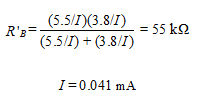
and
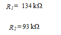
The design is therefore complete.
APPLICATION
Also, you can carry out these calculations with TINA or TINACloud circuit simulators, using their Interpreter tool by clicking the link below.