
2. Metal-oxide Semiconductor FET (MOSFET)
 CURRENT – 2. Metal-oxide Semiconductor FET (MOSFET)
 PREVIOUS- 1. Advantages and Disadvantages of FETs
Metal-oxide Semiconductor FET (MOSFET)
The metal-oxide semiconductor FET (MOSFET) is a four terminal device. The terminals are the source (S), gate (G) and drain (D). The substrate or body forms the fourth terminal. The MOSFET is constructed with the gate terminal insulated from the channel with a silicon dioxide dielectric. MOSFETs can be either depletion or enhancement mode. We define these two terms shortly.
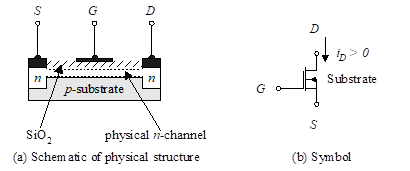
Figure 1 – n-channel depletion MOSFET
MOSFETs are sometimes referred to as IGFETs (Insulated Gate Field-Effect Transistors) due to the SiO2 layer used as an insulator between the gate and the substrate. We begin our analysis with the depletion-mode MOSFET. Just as BJTs can be either npn or pnp, MOSFETs can be either n-channel (NMOS) or p-channel (PMOS). Figure 1 illustrates the physical structure and symbol for an n-channel depletion MOSFET. Notice that the substrate is connected to the source terminal. This will almost always be the case.
The depletion MOSFET is constructed with a physical channel inserted between the drain and the source. As a result, when a voltage, vDS, is applied between drain and source, a current, iD, exists between drain and source even though the gate terminal G remains unconnected (vGS = 0 V).
The construction of the n-channel depletion MOSFET begins with p-doped silicon. The n-doped source and drain wells form low-resistance connections between the ends of the n-channel, as shown in the Figure 1. A thin layer of silicon dioxide is deposited covering the area between the source and the drain. The SiO2 is an insulator. An aluminum layer is deposited on the silicon dioxide insulator to form the gate terminal. In operation, a negative vGS pushes electrons out of the channel region, thereby depleting the channel. When vGS reaches a certain voltage, VT, the channel is pinched off. Positive values of vGS increase the channel size, resulting in an increase of drain current. The depletion MOSFET can operate with either positive or negative values of vGS. Since the gate is insulated from the channel, the gate current is negligibly small (on the order of 10-12 A).
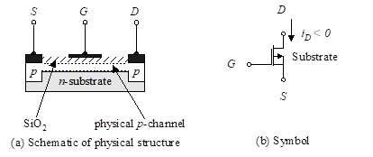
Figure 2 – p-channel depletion MOSFET
Figure 2 is comparable to Figure 1, except that we have changed the n-channel depletion MOSFET to a p-channel depletion MOSFET.
The n-channel enhancement MOSFET is illustrated in Figure 3 along with the circuit symbol. This is the most commonly used form of field-effect transistor.
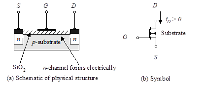
Figure 3 – n-channel enhancement MOSFET
The n-channel enhancement MOSFET differs from the depletion MOSFET by not having the thin n-layer. It requires a positive voltage between the gate and the source to establish a channel. This channel is formed by the action of a positive gate-to-source voltage, vGS, which attracts electrons from the substrate region between the n-doped drain and the source. Positive vGS causes electrons to accumulate at the surface beneath the oxide layer. When the voltage reaches a threshold, VT, sufficient numbers of electrons are attracted to this region to make it act like a conducting n-channel. No appreciable drain current, iD exists until vGS exceeds VT.
Figure 4 is comparable to Figure 3, except that we have changed the n-channel enhancement MOSFET to a p-channel enhancement MOSFET.
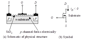
Figure 4 – p-channel enhancement MOSFET
As a summary, the MOSFET family exhibits the identifying iD versus vGS curves shown in Figure 5. Each characteristic curve is developed with sufficient drain-source voltage vDS to maintain the device in the normal operating region of the iD versus vDS curves. The discussion in later sections will define the threshold voltage VT for both enhancement MOSFETs and depletion MOSFETs.
Figure 5 – iD versus vGS characteristics of the MOSFET family for sufficient drain source voltage VDS
2.1 Enhancement-Mode MOSFET Terminal Characteristics
Now that we have presented the basic structure and basis for operation of the MOSFET, we use an approach in order to examine the terminal behavior of the enhancement-mode device. Let’s first make some general observations from Figure 1. Think of the normal flow of current in the MOSFET as being from the drain to the source (just as in the BJT, it is between collector and emitter). As with the npn BJT, two back-to-back diodes exist between drain and source. Therefore, we must apply external voltages to the gate in order to allow current to flow between the drain and the source.
If we ground the source, and apply a positive voltage to the gate, that voltage is effectively the gate-to-source voltage. The positive gate voltage attracts electrons and repels holes. When the voltage exceeds the threshold (VT), enough electrons are attracted to form a conducting channel between drain and source. At this point, the transistor turns on and the current is a function of both vGS and vDS. It should be clear that VT is a positive number for an n-channel device, and a negative number for a p-channel device.
Once a channel is created (i.e., vGS >VT), current flow can occur in that channel between drain and source. This current flow depends on vDS, but it also depends on vGS. When vGS just barely exceeds the threshold voltage, very little current can flow. As vGS increases beyond the threshold, the channel contains more carriers and higher currents are possible. Figure 6 shows the relationship between iD and vDS where vGS is a parameter. Note that for vGS less than the threshold, no current flows. For higher vGS, the relationship between iD and vDS is approximately linear indicating that the MOSFET behaves like a resistor whose resistance depends on vGS.
Figure 6 –iD versus vDS for an enhancement-mode n-channel MOSFET when vDS is small
The curves of Figure 6 look like straight lines. However, they will not continue as straight lines when vDS gets larger. Recall that a positive gate voltage is used to create the conduction channel. It does this by attracting electrons. The positive drain voltage is doing the same thing. As we approach the drain end of the channel, the voltage creating the channel approaches vGS–vDS since the two sources oppose each other. When this difference is less than VT, the channel no longer exists for the entire space between source and drain. The channel is constrained at the drain end, and further increases in vDS do not result in any increase in iD. This is known as the normal operating region or saturation region shown in Figure 7 by the horizontal section of the characteristic curves. When the difference is greater than VT, we call this the triode mode, because the potentials at all three terminals strongly affect the current.
The previous discussion leads to the operating curves of Figure 7.
Figure 7 –iD versus vGS for an enhancement-mode MOSFET
The transition between the triode and the normal operating region (referred to as the saturation region and often identified as operation in the pinch-off mode) of operation is shown as the dashed line in Figure 7, where
![]()
(1)
At the triode region border, the knees of the curves approximately follow the relationship,
![]()
(2)
In Equation (2), K is a constant for a given device. Its value depends on the dimensions of the device and the materials used in its construction. The constant is given by,
![]()
(3)
In this equation, μn is the electron mobility; Coxide, the oxide capacitance, is the capacitance per unit area of the gate; W is the width of the gate; L is the length of the gate. Equation indicates a complicated and nonlinear relationship between iD and the two voltages, vDS and vGS. Since we would like drain current to vary approximately linearly with vGS (independent of vDS), the FET is not generally used in the triode region.
We now wish to find an equation for the operating curves in the saturation region. We can establish the values at the transition between the triode and saturation region by evaluating Equation (2) at the transition (knee). That is,
![]()
(4)
This equation establishes the magnitude of the drain current at the boundary (dashed line in Figure 8) as a function of the gate-to-source voltage vGS. If necessary, we can account for the slight slope of the characteristic curves in the saturation region by adding a linear factor.
![]()
(5)
In Equation (5) , λ is a small constant (the slope of the near horizontal section of the characteristic curves shown in Figure 8). It is usually less than 0.001 (V-1). Then
![]()
(6)
All of our previous discussion dealt with the NMOS transistor. We now briefly discuss the necessary modifications for PMOS. For PMOS, the values of vDS will be negative. Additionally, to create a channel in PMOS, ![]() .
.
Figure 8 – Terminal characteristics of a MOSFET transistor
The only changes from the characteristics of NMOS transistors (Figure 7) is that the horizontal axis is now -vDS instead of +vDS, and the parametric curves represent higher drain current as the gate voltage decreases (instead of increasing for the NMOS transistor). The curves for increasing current values correspond to more negative gate voltage. When vGS > VT, the transistor is cut-off. For enhancement PMOS, VT is negative, and for depletion PMOS, VT is positive.
The equation for the current at the triode region transition for the PMOS transistor is identical to that of the NMOS. That is,
![]()
(7)
Note that vGS and vDS are both negative quantities. The equation for the saturation region in the PMOS transistor is also identical to that of the NMOS. That is,
![]()
(8)
Note that λ is negative for PMOS transistors since the rate of change of the curve (![]() ) is negative.
) is negative.
Taking the partial derivative of both sides of Equation (6) with respect to vGS, ![]() , we get
, we get
![]()
(9)
We prefer the value of gm to be constant, especially for large signal swings. However, we only can approximate this condition if we use the FET for small signal applications. For large signal conditions, distortion of the waveform may be unacceptable in some applications.
2.2 Depletion-Mode MOSFET
The previous section dealt with the enhancement-mode MOSFET. We now contrast this to the depletion-mode MOSFET. For the n-channel enhancement mode, to acquire a channel we had to apply a positive voltage on the gate. This voltage had to be large enough to force sufficient numbers of mobile electrons to produce a current in an induced channel.
Figure 9 – Depletion mode n-channel MOSFET
In the n-channel depletion-mode MOSFET, we don’t need this positive voltage since we have a physically implanted channel. This allows us to have current between the drain and source terminals even with negative voltages applied to the gate. Of course, there is a limit to the amount of negative voltage that can be applied to the gate while still having current flow between drain and source. This limit is again identified as the threshold voltage, VT. The change from the enhancement mode is that the gate-to-source voltage can now be either negative or positive, as shown in Figure 9.
The equations that define the operation of the depletion- mode MOSFET are very similar to those of the enhancement mode. The value of the drain current when vGS is zero is identified as IDSS. This is often referred to as the drain-source saturation current, or the zero – gate drain current. Comparing the equations of the enhancement-mode MOSFET with those of the depletion mode, we find
![]()
(10)
We then find,
![]()
(11)
Depletion mode MOSFETs are available in discrete form, or they can be fabricated on integrated circuits chips right along with enhancement mode types. This includes both p-type and n-type. This allows more flexibility in circuit design techniques.
2.3 Large-signal equivalent circuit
We now wish to develop an equivalent circuit which represents the large-signal characteristics of Figure 8 [Equation (5) or (8) ] in the saturation region. Note that the drain current, iD, depends on vGS and vDS. For a constant gate-to-source voltage, we operate along one of the parametric curves of the figure, and the relationship is an approximately straight line. A straight-line relationship between current and voltage is modeled by a resistor. The equivalent circuit therefore consists of a resistor in parallel with the current source where the value of the current source establishes the portion of the drain current due to vGS. The slope of the curve depends on vGS. The slope is the partial derivative,
![]()
(12)
where r0 is the incremental output resistance. We see from Equation [ (5) or (8) ] that this resistance is given by
![]()
(13)
where we use upper-case VGS to indicate that the resistance is defined for a particular constant value of gate-to-source voltage. The final approximation in Equation (13) results from Equation (5) with the assumption that λ is small. The resistance is therefore inversely proportion to the bias current, ID. The large signal equivalent model is then given by Figure 11 where r0 is as developed in Equation (13).
Figure 11 – Large-signal equivalent circuit
2.4 Small-Signal Model of MOSFET
We now wish to look at incremental effects related to Equation . The three circuit parameters in that equation, iD, vGS and vDS are composed of both dc (bias) and ac components (that is why we have used upper case subscripts in the expressions). We are interested in the ac components for the small-signal model. We see that the drain current is dependent on two voltages, the gate-to-source and the drain-to-source. For incremental values, we can write this relationship as
![]()
(14)
In Equation (14), gm is the forward transconductance and r0 is the output resistance. Their values are found by taking partial derivatives in Equation (5). Thus,
![]()
(15)
The approximation in Equation (15) results from the observation that λ if small. Equation (14) leads to the small-signal model of Figure 12.
Figure 12 – Small-signal MOSFET model