
9. FET Amplifier analysis
 CURRENT – 9. FET Amplifier analysis
 PREVIOUS- 8. FET Amplifiers – Canonical configurations
FET Amplifier analysis
9.1 The CS (and Source Resistor) Amplifier
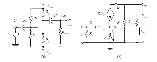
Figure 33 – The CS amplifier with source resistor
Figure 33(a) shows the CS amplifier with source resistor. The ac equivalent circuit is in Figure 33(b). We assume ro is large compared to , so it can be neglected. If a capacitor is present between source and ground (i.e., the CS amplifier), we need simply set RS equal to zero in the following ac equations. We do this at the conclusion of this derivation.
In part (b) of Figure 33, RG is the parallel combination of R1 and R2 and VGG is the Thevenin equivalent voltage of the bias circuit:
![]() (41)
(41)
To analyze the ac equivalent circuit, we write a KVL equation around the gate circuit.
![]() (42)
(42)
The output voltage, vout, is given by
![]()
The voltage gain, Av, is now found.
![]() (43)
(43)
If the source resistance, RS, is bypassed by a capacitor, we let RS = 0, and the voltage gain increases to
![]() (44)
(44)
This is typically a large negative number.
The input resistance and current gain are given by
![]() (45)
(45)
9.2 The CG Amplifier
Figure 37(a) shows the single-stage common-gate amplifier and Figure 6.37(b) shows its ac equivalent. We have once again neglected ro under the assumption that it is large compared to the parallel combination of RD with Rload.
Figure 37 – CG amplifier
From Figure 37(b) leftmost loop, the gate-to-source voltage is given by
![]() (46)
(46)
The current through RS is
![]() (47)
(47)
so the (input) resistance seen by the source is
![]() (48)
(48)
This should be compared to Equation (45) for the CS amplifier. We see that if the gate resistance is high, the input resistance of the common-source amplifier can be much larger than that of the common-gate amplifier. In fact, the number of applications of the CG amplifier is limited due to the low input impedance.
The voltage gain is given by
![]() (49)
(49)
Comparing this with Equation (44) , we see that the voltage gain for the CS amplifier with an unbypassed resistance in the source circuit is the same as that of the CG amplifier except the CG amplifier does not shift the phase.
The output resistance is simply given by RD (put in a test current and measure the voltage while setting vin to zero).
The current gain of the CG amplifier is
![]() (50)
(50)
9.3 The CD (SF) Amplifier
Figure 39(a) shows the single-stage common-drain source follower (SF) amplifier and Figure 39(b) shows its ac equivalent. As with each configuration we have analyzed, we omit the large resistance, ro under the assumption it is much larger than the parallel combination of RS with Rload.
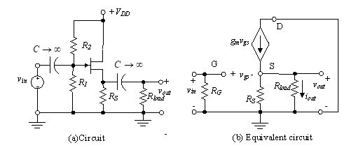
Figure 39 – The CD amplifier
The input resistance is simply Rin = RG. Writing a KVL equation around the gate-to-source loop, we have
![]() (51)
(51)
from which we obtain
![]() (52)
(52)
The output voltage is
![]() (53)
(53)
The voltage gain is the ratio of output to input voltage.
![]() (54)
(54)
Note that this voltage gain is less than unity, and it approaches one as the parallel combination of RS with Rload increases.
We now find the current gain. The output current is the ratio of the output voltage to the load resistance. The input current is the input voltage divided by RG. The gain is therefore given by
![]() (55)
(55)
The output resistance can be found by replacing the load resistor with a test voltage, vtest, and then finding the resulting current, itest. The current driven by this test source is found from a node equation at the source.
![]() (56)
(56)
The gate-to-source voltage is simply -vtest since we assume the input voltage is zero. Therefore, the output resistance is
![]() (57)
(57)