10. FET Amplifier design
 CURRENT – 10. FET Amplifier design
 PREVIOUS- 9. FET Amplifier analysis
FET Amplifier design
We now explore the extension of the FET amplifier analysis presented earlier in this chapter to the design of FET amplifiers. We will attempt to define the unknowns in the design problem, and then develop equations for solving for these unknowns. As in most electronics design, the number of equations will be less than the number of unknowns. The additional constraints are established to meet certain overall objectives (e.g., minimum cost, less variation in performance due to parameter changes).
10.1 The CS Amplifier
The design procedure of a CS amplifier is presented in this section. We shall reduce JFET and the depletion MOSFET amplifier design to an organized procedure. While this may appear to
reduce design to a very routine process, you must convince yourself that you understand the origin of each step since several variations may be subsequently required. If all you do to design a CS amplifier is to thoughtlessly “plug in” to the steps we present, you are missing the whole point of this discussion. As an engineer, you are seeking to do things that are not routine. Reducing theory to an organized approach is what you will be doing. You will not simply apply the approaches others have already done for you.
Amplifiers are designed to meet gain requirements assuming the desired specifications are within the range of the transistor. The supply voltage, load resistance, voltage gain and input resistance (or current gain) are usually specified. The designer’s job is to select the resistance values R1, R2, RD, and RS. Refer to Figure 40 as you follow the steps in the procedure. This procedure assumes that a device has been selected and that its characteristics are known.
Figure 40 JFET CS amplifier
First, select a Q-point in the saturation region of the FET characteristic curves. Refer to the curves of Figure 40(b) for an example. This identifies VDSQ, VGSQ, and IDQ.
We now solve for the two resistors in the output loop, RS and RD. Since there are two unknowns, we require two independent equations. We begin by writing the dc KVL equation around the drain-source loop,
![]() (58)
(58)
Solving for the sum of the two resistors yields
![]() (59)
(59)
![]() (60)
(60)
The resistance, RD, is the only unknown in this equation. Solving for RD results in a quadratic equation having two solutions, one negative and one positive. If the positive solution results in RD > K1, thus implying a negative RS, a new Q-point must be selected (i.e., restart the design). If the positive solution yields RD < K1, we can proceed.
Now that RD is known, we solve for RS using Equation (59) , the drain-to-source loop equation.
![]() (61)
(61)
With RD and RS known, we need only find R1 and R2.
We begin by rewriting the KVL equation for the gate-source loop.
![]() (62)
(62)
The voltage, VGS, is of opposite polarity from VDD. Thus the term IDQRS must be greater than VGSQ in magnitude. Otherwise, VGG will have the opposite polarity from VDD, which is not possible according to Equation (62).
We now solve for R1 and R2 assuming that the VGG found has the same polarity as VDD. These resistor values are selected by finding the value of RG from the current-gain equation or from the input resistance. We solve for R1 and R2.
![]() (63)
(63)
Suppose now that Equation (62) results in a VGG that has the opposite polarity of VDD. It is not possible to solve for R1 and R2. The practical way to proceed is to let VGG = 0 V. Thus, ![]() . Since VGG is specified by Equation (62) , the previously calculated value of RS now needs to be modified.
. Since VGG is specified by Equation (62) , the previously calculated value of RS now needs to be modified.
Figure 41 – CS amplifier
In Figure 41, where a capacitor is used to bypass a part of RS, we develop the new value of RS as follows:
![]() (64)
(64)
The value of RSdc is RS1 + RS2 and the value of RSac is RS1.
Now that we have a new RSdc, we must repeat several earlier steps in the design. We once again determine RD using KVL for the drain-to-source loop.
![]() (65)
(65)
The design problem now becomes one of calculating both RS1 and RS2 instead of finding only one source resistor.
With a new value for RD of K1 – RSdc, we go to the voltage gain expression of Equation (60) with RSac used for this ac equation rather than RS. The following additional steps must be added to the design procedure:
We find RSac (which is simply RS1) from the voltage gain equation
![]() (66)
(66)
RSac is the only unknown in this equation. Solving for this, we find
![]() (67)
(67)
Suppose now that RSac is found to be positive, but less than RSdc. This is the desirable condition since
![]() (68)
(68)
Then our design is complete and
![]() (69)
(69)
Suppose that RSac is found to be positive but greater than RSdc. The amplifier cannot be designed with the voltage gain and Q-point as selected. A new Q-point must be selected. If the voltage gain is too high, it may not be possible to effect the design with any Q-point. A different transistor may be needed or the use of two separate stages may be required.
10.2 The CD Amplifier
We now present the design procedure for the CD JFET amplifier. The following quantities are specified: current gain, load resistance, and VDD. Input resistance may be specified instead of current gain. Refer to the circuit of Figure 39 as you study the following procedure. Once again, we remind you that the process of reducing the theory to a set of steps is the important part of this discussion – not the actual steps.
First select a Q-point in the center of the FET characteristic curves with the aid of Figure 20 (“Chapter 3: Junction field-effect transistor (JFET)”). This step determines VDSQ, VGSQ, IDQ and gm.
We can solve for the resistor connected to the source by writing the dc KVL equation around the drain-to-source loop.
![]() (70)
(70)
from which we find the dc value of RS,
![]() (71)
(71)
We next find the ac value of resistance, RSac, from the rearranged current gain equation, Equation (55).
![]() (72)
(72)
where RG = Rin. If the input resistance is not specified, let RSac = RSdc and calculate the input resistance from Equation (72) . If the input resistance is not high enough, it may be necessary to change the Q-point location.
If Rin is specified, it is necessary to calculate RSac from Equation (72). In such cases, RSac is different from RSdc, so we bypass part of RS with a capacitor.
We now turn our attention to the input bias circuitry. We determine VGG using the equation,
![]() (73)
(73)
No phase inversion is produced in a source follower FET amplifier and VGG is normally of the same polarity as the supply voltage.
Now that VGG is known, we determine the values of R1 and R2 from the Thevenin equivalent of the bias circuitry
![]() (74)
(74)
There is usually enough drain current in an SF to develop the opposite polarity voltage needed to offset the negative voltages required by the JFET gate. Therefore, normal voltage division biasing can be used.
Figure 44 – CD amplifier with part of RS bypassed
We now return to the problem of specifying the input resistance. We can assume that part of RS is bypassed, as in Figure 44, which leads to different values of RSac and RSdc. We use Equation (71) to solve for RSdc. Next, we let RG equal the specified value of Rin, and use Equation (72) to solve for RSac.
If the RSac calculated above is smaller than RSdc, the design is accomplished by bypassing RS2 with a capacitor. Remember that RSac = RS1 and RSdc = RS1 + RS2. If on the other hand, RSac is larger than RSdc, the Q-point must be moved to a different location. We select a smaller VDS thus causing increased voltage to be dropped across RS1 + RS2, which makes RSdc larger. If VDS cannot be reduced sufficiently to make RSdc larger than RSac, then the amplifier cannot be designed with the given current gain, Rin, and FET type. One of these three specifications must be changed, or a second amplifier stage must be used to provide the required gain.
10.3 The SF Bootstrap Amplifier
We now examine a variation of the CD amplifier known as the SF (or CD) bootstrap FET amplifier. This circuit is a special case of the SF called the bootstrap circuit and is illustrated in Figure 45.
Here the bias is developed across only a part of the source resistor. This reduces the need for a capacitor bypass across part of the source resistor and thus attains a much larger input resistance than normally can be attained. This design allows us to take advantage of the high impedance characteristics of the FET without using a high value of gate resistor, RG.
The equivalent circuit of Figure 46 is used to evaluate the circuit operation
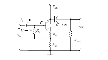
Figure 45 – Bootstrap source follower
We assume that iin is sufficiently small to approximate the current in RS2 as i1. The output voltage is then found to be
![]() (75)
(75)
where
![]() (76)
(76)
If the assumption about iin is not valid, is replaced by the expression
![]() (77)
(77)
A KVL equation at the input yields vin as follows:
![]() (78)
(78)
The current, i1, is found from a current-divider relationship,
![]() (79)
(79)
Combining Equations (79) and (78) yields,
![]() (80)
(80)
A second equation for vin is developed around the loop through RG and RS2 as follows.
![]() (81)
(81)
We eliminate vin by setting Equation (80) equal to Equation (81) and solve for iin to obtain
![]() (82)
(82)
The input resistance, Rin = vin/iin, is found by dividing Equation (81) by Equation (82) with the result,
![]() (83)
(83)
RG is the only unknown in this equation, so we can solve to obtain,
![]() (84)
(84)
The current gain is
![]() (85)
(85)
We can now use the equations derived earlier along with the observation that RS – RS2 = RS1 in order to solve for the current gain.
![]() (86)
(86)
The voltage gain is
![]() (87)
(87)
Note that the denominator in Equation (84) is larger than the numerator, thus showing that RG < (Rin–RS2). This proves that a large input resistance can be attained without having the same order of size as RG.