
4. FET Amplifier Configurations and Biasing
 CURRENT – 4. FET Amplifier Configurations and Biasing
 PREVIOUS- 3. Junction Field-effect Transistor (JFET)
FET Amplifier Configurations and Biasing
The approaches that are used for biasing of BJTs can also be used for biasing MOSFETS. We can separate the approaches into those used for discrete component versus integrated circuit amplifiers. Discrete component designs use the large coupling and bypass capacitors to isolate the dc bias for each amplifier stage, much like the discrete component BJT amplifiers. IC MOSFET amplifiers are generally direct coupled because large capacitors are not practical. The IC MOSFET amplifiers are usually biased using dc current sources that are analogous to those used for the BJT IC amplifiers.
4.1 Discrete-Component MOSFET Biasing
Discrete-component biasing for MOSFET amplifiers is accomplished with the circuits shown in Figure 21. The gate-to-source voltage determines the type of circuit which may be required for that transistor configuration. For an enhancement mode transistor, there will always be a need for a positive voltage at the gate. In the voltage division biasing, there will be an R1 and R2 in order to obtain the positive voltage. For depletion MOSFETs or JFETs, R2 can either be finite or infinite, as shown in Figure 21(b).
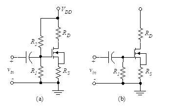
Figure 21 – Amplifier biasing configurations
Common Source (CS)– the ac input is applied at CG, the ac output is taken at CD, and CS is connected to a dc voltage source or ground. This is analogous to the common-emitter configuration for the BJT.
–Source Resistor (SR) – the ac input is applied at CG, the ac output is taken at CD and CS is omitted. This is analogous to the emitter-resistor configuration for the BJT.
–Common Gate (CG) – the ac input is applied at CS, the ac output is taken at CD and CG is connected to a dc voltage source or ground. Sometimes in the CG configuration, CG is omitted and the gate is connected directly to a dc voltage supply. The CG is analogous to the common base configuration for the BJT, although it is seldom seen in circuits.
–Source Follower (SF) – the ac input is applied at CG, the ac output is taken at CS and the drain is either connected to a dc voltage supply directly or via CD. This is sometimes called common drain (CD) and is analogous to the emitter follower configuration for the BJT.
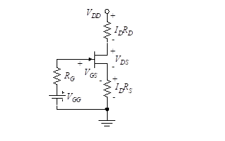
Figure 22 – Thevenin equivalent circuit
Each of these configurations is studied in more detail in Section 9, “FET Amplifier analysis”.
Since the different configurations only vary in their connections via the capacitors, and the capacitors are open circuits to dc voltages and currents, we can study the dc bias for the general case. For amplifier design, we want the transistor to operate in the active operating region (also identified as the saturation region or pinch-off mode), so we assume the pinch-off I-V characteristic for the device. (We should always verify this assumption at the end of the design!)
To simplify the bias analysis, we use a Thevenin source to model the circuit at the gate of the transistor as shown in Figure 22.
![]()
(24)
Since there are three unknown variables to set for biasing (ID, VGS, and VDS), we need three dc equations. First, the dc equation around the gate-source loop is written.
![]()
(25)
Notice that since the gate current is zero, a zero voltage drop exists across RG. A second dc equation is found from the Kirchhoff’s law equation in the drain-source loop.
![]()
(26)
The third dc equation necessary to establish the bias point is found from Equation (20) ![]() in section ” Junction field-effect transistor (JFET)” which is repeated here.
in section ” Junction field-effect transistor (JFET)” which is repeated here.
![]()
(27)
The first approximation applies if |λVDS| << 1 (which is nearly always true) and simplifies the solution of the coupled equations considerably.
We can put the equation for gm [Equation (22)]
![]()
(22)
into a similar format that will prove useful in design.
![]()
(28)
Equations (25)-(28) are sufficient to establish the bias. For discrete MOSFET amplifiers, we do not need to put the Q-point in the center of the ac load line as we often did for BJT biasing. This is because discrete FET amplifiers are normally used as the first stage in an amplifier chain to take advantage of the high input resistance. When used as a first stage or preamplifier, the voltage levels are so small that we do not drive the output of the preamplifier over large excursions.