
7. Other Op-amp Applications
 CURRENT – 7. Other op-amp applications
 PREVIOUS- 6. Design of op-amp circuits
Other op-amp applications
We have seen that the op-amp can be used as an amplifier, or as a means of combining a number of inputs in a linear manner. We now investigate several additional important applications of this versatile linear IC.
7.1 Negative Impedance Circuit
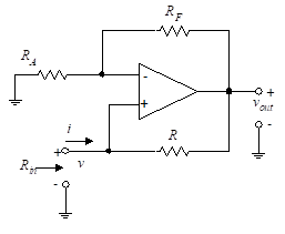
Figure 17 Negative Impedance Circuit
The circuit shown in Figure (17) produces a negative input resistance (impedance in the general case).
This circuit can be used to cancel an unwanted positive resistance. Many oscillator applications depend on a negative resistance op-amp circuit. The input resistance, Rin, is the ratio of input voltage to current.
![]()
(43)
A voltage divider relationship is used to derive the expression for v– since the current into the op-amp is zero.
![]()
(44)
We now let v+ = v– and solve for vout in terms of vin, which yields,
![]()
(45)
Since the input impedance to the v+ terminal is infinite, the current in R is equal to iin and can be found as follows:
![]()
(46)
The input resistance, Rin, is then given by
![]()
(47)
Equation (47) shows that the circuit of Figure (17) develops a negative resistance. If R is replaced by an impedance, Z, the circuit develops a negative impedance.
APPLICATION
Analyze the following circuit online with the TINACloud circuit simulator by clicking the link below.
1- Negative Impedance Circuit Simulation
7.2 Dependent-Current Generator
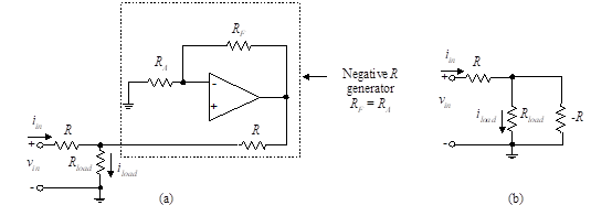
Figure 18 – Dependent current generator
Suppose we let RF = RA. Equation (47)then indicates that the input resistance to the op-amp circuit (enclosed in the dashed box) is -R. The input circuit can then be simplified as shown in Figure 18(b). We wish to calculate iload, the current in Rload. Although the resistance is negative, the normal Kirchhoff’s laws still apply since nothing in their derivations assumes positive resistors. The input current, iin, is then found by combining the resistances into a single resistor, Rin.
![]()
(48)
We then apply a current-divider ratio to the current split between Rload and -R to obtain
![]()
(49)
Thus the effect of the addition of the op-amp circuit is to make the current in the load proportional to the input voltage. It does not depend upon the value of the load resistance, Rload. The current is therefore independent of changes in the load resistance. The op-amp circuit effectively cancels out the load resistance. Since the current is independent of the load but depends only upon the input voltage, we call this a current generator (or voltage-to-current converter).
Among the many applications of this circuit is a dc regulated voltage source. If we let vin = E (a constant), the current through Rload is constant independent of variations of Rload.
APPLICATION
Analyze the following circuit online with the TINACloud circuit simulator by clicking the link below.
2- Dependent Current Generator Circuit Simulation
7.3 Current-to-Voltage Converter
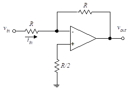
Figure 19 – Current -to-Voltage converter
The circuit of Figure (19) produces an output voltage that is proportional to the input current (this can also be viewed as a unity-gain inverting amplifier). We analyze this circuit in using the properties of ideal op-amps. We solve for the voltages at the input terminals to find
![]()
(50)
Hence, the output voltage, vout = -iinR, is proportional to the input current, iin.
APPLICATION
Analyze the following circuit online with the TINACloud circuit simulator by clicking the link below.
3- Current to Voltage Converter Circuit Simulation
7.4 Voltage-to-Current Converter
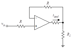
Figure 20 – Voltage to current converter
The circuit of Figure (20), is a voltage-to-current converter. We analyze this circuit as follows:
![]()
(51)
From Equation (51) we find,
![]()
(52)
Therefore, the load current is independent of the load resistor, Rload, and is proportional to the applied voltage, vin. This circuit develops a voltage-controlled current source. However, a practical shortcoming of this circuit is that neither end of the load resistor can be grounded.
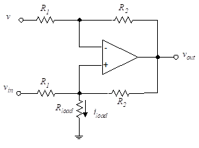
Figure 21 – Voltage-to-current converter
We analyze this circuit by writing node equations as follows:
(53)
The last equality uses the fact that v+ = v–. There are five unknowns in these equations (v+, vin, vout, v, and iload). We eliminate v+ and vout to obtain,
![]()
(54)
The load current, iload, is independent of the load, Rload, and is only a function of the voltage difference, (vin – v).
APPLICATION
Analyze the following circuit online with the TINACloud circuit simulator by clicking the link below.
4-Voltage to Current Converter Circuit Simulation
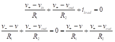
7.5 Inverting Amplifier with Generalized Impedances
Figure 22 – Use of generalized impedance in place of resistance
The relationship of Equation (17) is easily extended to include non-resistive components if Rj is replaced by an impedance, Zj, and RF is replaced by ZF. For a single input, as shown in Figure 22 (a), the output reduces to
![]()
(55)
Since we are dealing in the frequency domain, we use uppercase letters for the voltages and currents, thus representing the complex amplitudes.
One useful circuit based on Equation (55) is the Miller integrator, as shown in Figure 22(b). In this application, the feedback component is a capacitor, C, and the input component is a resistor, R, so
![]()
(56)
In Equation (56) , s is the Laplace transform operator. For sinusoidal signals, ![]() . When we substitute these impedances into Equation (55) , we obtain
. When we substitute these impedances into Equation (55) , we obtain
![]()
(57)
In the complex frequency domain, 1/s corresponds to integration in the time domain. This is an inverting integrator because the expression contains a negative sign. Hence the output voltage is
![]()
(58)
where vout(0) is the initial condition. The value of vout is developed as the voltage across the capacitor, C, at time t = 0. The switch is closed to charge the capacitor to the voltage vout(0) and then at t = 0 the switch is open. We use electronic switches, which we discuss more fully in Chapter 16. In the event that the initial condition is zero, the switch is still used to reset the integrator to zero output voltage at time t = 0.
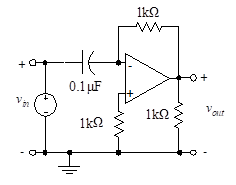
Figure 23 – Example of an inverting differentiator
If the feedback element is a resistor, and the input element is a capacitor, as shown in Figure (23), the input-output relationship becomes
![]()
(59)
In the time domain, this becomes
![]()
(60)
APPLICATION
Analyze the following circuit online with the TINACloud circuit simulator by clicking the link below.
5- Example of an inverting differentiator Circuit Simulation
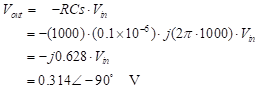
The circuit is operating as an inverting differentiator. Note that the input capacitor, Za = 1/sC, does not provide a path for dc. This does not affect the result since the derivative of a constant is zero. For simplicity, let’s use a sinusoidal input signal. Rearranging Equation (59) and substituting the numeric values for this circuit, we obtain
(61)
The input voltage is inverted (180° shift) by this circuit and then scaled and shifted again (90° by the j-operator) by the value of RCs where ![]() .
.
Results of the simulation are shown in Figure (24).
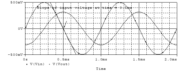
Figure 24 – Simulation results for inverting differentiator
The input waveform peaks at 0.5 volts. The output voltage has a net shift (delay) of 90 degrees and the output voltage peaks at approximately 0.314 volts. This is in good agreement with the result of Equation (61) .
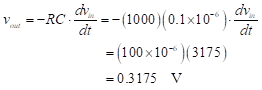
We may also use the waveforms to show that this circuit performs the task of an inverting differentiator. We will confirm that the output waveform represents the slope of the input signal times a constant. The constant is the voltage gain of the circuit. The greatest rate of change of the input voltage waveform occurs at its zero-crossing. This corresponds with the time that the output waveform reaches its maximum (or minimum). Picking a representative point, say at time0.5 ms, and using graphical techniques, we compute the slope of the input voltage waveform as
![]()
(62)
Scaling this rate of change (i.e.,![]() ) by the circuit voltage gain according to Equation (60)we expect the peak output voltage to be
) by the circuit voltage gain according to Equation (60)we expect the peak output voltage to be
(63)
7.6 Analog Computer Applications
In this section we present the use of interconnected op-amp circuits, such as summers and integrators, to form an analog computer which is used to solve differential equations. Many physical systems are described by linear differential equations, and the system can therefore be analyzed with the aid of an analog computer.
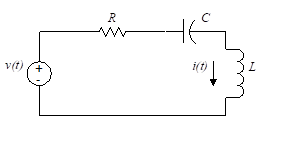
Figure 25 – Analog computer application
Let us solve for the current, i(t), in the circuit of Figure 25. The input voltage is the driving function and the initial conditions are zero. We write the differential equation for the circuit as follows:
![]()
(64)
Now solving for di/dt, we obtain
![]()
(65)
We know that for t > 0,
![]()
(66)
From Equation (65) we see that -di/dt is formed by summing three terms, which are found on Figure 26 at the input to the first integrating amplifier.
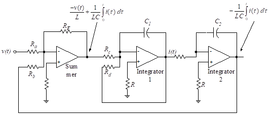
Figure 26 – Analog computer solution for Figure 25
The three terms are found as follows:
1. The driving function, -v(t)/L, is formed by passing v(t) through an inverting summer (Summer) with gain, 1/L.
2. Ri/L is formed by taking the output of the first integrating amplifier (Integrator 1) and adding it at the amplifier input to the output of the summing amplifier (Summer).
3. The term
![]()
(67)
is the output of the second integrator (Integrator 2). Since the sign must be changed, we sum it with the unity gain inverting summer (Summer).
The output of the first integrator is +i, as seen from Equation (66). The constants in the differential equation are established by proper selection of the resistors and capacitors of the analog computer. Zero initial conditions are accomplished by switches across the capacitors, as shown in Figure 22(b).
7.7 Non-Inverting Miller Integrator
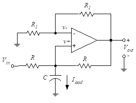
Figure 27 – Non-inverting integrator
We use a modification of the dependent current generator of the previous section to develop a non-inverting integrator. The circuit is configured as shown in Figure 27.
This is similar to the circuit of Figure 21, but the load resistance has been replaced by a capacitance. We now find the current, Iload. The inverting voltage, V-, is found from the voltage division between Vo and V- as follows:
(68)
Since V+ = V-, we solve and find
IL = Vin /R. Note that
![]()
(69)
where s is the Laplace transform operator. The Vout /Vin function is then
![]()
(70)
Thus, in the time domain we have
![]()
(71)
The circuit is therefore a non-inverting integrator.
APPLICATION
Analyze the following circuit online with the TINACloud circuit simulator by clicking the link below.
6-Non-inverting integrator Circuit Simulation
SUMMARY
The operational amplifier is a very useful building block for electronic systems. The real amplifier operates almost as an ideal amplifier with very high gain and almost infinite input impedance. For this reason, we can treat it in the same way we treat circuit components. That is, we are able to incorporate the amplifier into useful configurations prior to studying the internal operation and the electronic characteristics. By recognizing the terminal characteristics, we are able to configure amplifiers and other useful circuits.
This chapter began with an analysis of the ideal operational amplifier, and with development of equivalent circuit models using dependent sources. The dependent sources we studied early in this chapter form the building blocks of equivalent circuits for many of the electronic devices we study in this text.
We then explored the external connections needed to make the op-amp into an inverting amplifier, a non-inverting amplifier, and a multiple input amplifier. We developed a convenient design technique eliminating the need for solving large systems of simultaneous equations.
Finally, we saw how the op-amp could be used to build a variety of more complex circuits, including circuits which are equivalent to negative impedances (which can be used to cancel the effects of positive impedances), integrators and differentiators.