11. Other devices
 CURRENT – 11. Other devices
 PREVIOUS- 10. FET Amplifier design
Other devices
Other devices that are an outgrowth of the normal two- and three-terminal devices are presented in this section.
11.1 Metal Semiconductor Barrier Junction Transistor
The metal semiconductor barrier junction transistor (MESFET) is similar to a FET, except that the junction is a metal semiconductor barrier, much as is the case with Schottky diodes. FETs made of silicon (Si) or gallium arsenide (GaAs) are constructed with diffused or ion implanted gates. However, there are advantages to using a Schottky barrier metal gate when the channel is n-type and short channel widths are needed. Gallium arsenide (GaAs) is difficult to work with, yet it makes good Schottky barriers that are useful in high frequency applications because electrons travel faster in GaAs than in Si. Using GaAs in MESFETs results in a transistor that exhibits good performance in microwave applications. In comparison with the silicon bipolar transistor, GaAs MESFETs have better performance at input frequencies above 4 GHz. These MESFETs exhibit high gain, low noise, high efficiency, high input impedance, and properties that prevent thermal runaway. They are used in microwave oscillators, amplifiers, mixers, and also for high speed switching. GaAs MESFETs are used for high-frequency applications.
11.2 VMOSFET (VMOS)
Considerable research effort has been applied to increasing the power capability of solid state devices. An area that has shown much promise is the MOSFET where the conduction channel is modified to form a “V” rather than the conventional source-to-drain straight line. An additional semiconductor layer is added. The term VMOS is derived from the fact that the current between source and drain follows a vertical path due to the construction. The drain is now located on a piece of added semiconductor material, as illustrated in Figure 47. This allows the transistor drain area to be placed in contact with a heat sink to aid in dissipating the heat generated in the device. The V-shaped gate controls two vertical MOSFETs, one on each side of the notch. By parallelling the two S terminals, the current capacity can be doubled. VMOS is unsymmetrical so that the S and D terminals cannot be interchanged as is the case in low-power MOS FETs. Conventional FETs are limited to currents of the order of milliamperes, but VMOS FETs are available for operation in the 100A current range. This provides a great improvement in power over the conventional FET.
The VMOS device can provide a solution to high frequency, high power applications. Ten watt devices have been developed at frequencies in the lower ultra-high frequency (UHF) band. There are other important advantages of VMOS FETs. They have a negative temperature coefficient to prevent thermal runaway. Also they exhibit low leakage current. They are capable of achieving high switching speed. VMOS transistors can be made to have equal spacing of their characteristic curves for equal increments of gate voltage, so they can be used like bipolar junction transistors for high power linear amplifiers.
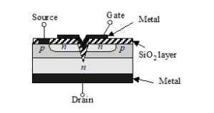
Figure 47 – VMOS construction
11.3 Other MOS Devices
Another type of MOS device is a double-diffused process fabricated FET sometimes called DMOS. This device has the advantage of decreasing the length of the channels, thus providing excellent low power dissipation and high speed capability.
Fabrication of a FET on small silicon islands on a substrate of sapphire is sometimes referred to as SOS. The islands of silicon are formed by etching a thin layer of silicon grown on the sapphire substrate. This type of fabrication provides insulation between the islands of silicon, thus greatly reducing parasitic capacitance between devices.
MOS technology has the advantage that both capacitors and resistors (using MOSFETs) are made at the same time as the FET, although large value capacitors are not feasible. Using an enhancement MOSFET, a two-terminal resistance is made and the MOSFET gate connected to the drain causes the FET to operate at pinch-off. The MOSFET gate is connected to the drain through a power source causing the FET to be biased where it will operate in the voltage-controlled resistance region of the characteristics. In this way, drain-load resistors are replaced by a MOSFET rather than a deposited resistor hence saving chip area.
SUMMARY
The purpose of this chapter was to introduce you to the analysis and design of amplifier circuits using field-effect transistors. The FET is quite different from the BJT. Its operation is controlled by a voltage as contrasted with the BJT which is a current-controlled device.
Our approach paralleled that of the BJT chapters. We began with an examination of the physical phenomena that govern FET behavior. In the process, we emphasized the contrast between FETs and BJTs. We began our study with MOSFETs and then turned our attention to JFETs. Also we developed small-signal models for these important devices. We used those models to analyze the various configurations of FET amplifiers. Once we knew how to analyze FET circuits, we turned our attention to design to meet specifications. We also examined the models used by computer simulation programs.
We briefly looked at the manner in which FETs are fabricated as part of integrated circuits. The chapter concluded with an introduction to other types of FET devices, including the MESFET and the VMOS.