
3. Junction Field-effect Transistor (JFET)
 CURRENT – 3. Junction Field-effect Transistor (JFET)
 PREVIOUS- 2. Metal-oxide semiconductor FET (MOSFET)
Junction Field-effect Transistor (JFET)
The MOSFET has a number of advantages over the junction field-effect transistor (JFET). Notably, the input resistance of the MOSFET is higher than that of the JFET. For this reason, the MOSFET is selected in favor of the JFET for most applications. Nonetheless, the JFET is still used in limited situations especially for analog applications.
We have seen that enhancement MOSFETs require a non-zero gate voltage to form a channel for conduction. No majority-carrier current can flow between the source and the drain without this applied gate voltage. In contrast, the JFET controls the conductance of majority-carrier current in an existing channel between two ohmic contacts. It does this by varying the equivalent capacitance of the device.
Although we approach JFETs without using the results derived earlier for MOSFETs, we will see many similarities in the operation of the two types of devices. These similarities are summarized in Section 6: “Comparison of MOSFET to JFET”.
A schematic for the physical structure of the JFET is shown in Figure 13. Like the BJT, the JFET is a three terminal device. It has basically only one pn junction between the gate and the channel rather than two as in the BJT (although there appear to be two pn junctions shown in Figure 13, these are connected in parallel by wiring the gate terminals together. They can thus be treated as a single junction).
The n-channel JFET, shown in Figure 14(a), is constructed using a strip of n-type material with two p-type materials diffused into the strip, one on each side. The p-channel JFET has a strip of p-type material with two n-type materials diffused into the strip, as shown in Figure 13(b). Figure 13 also shows the circuit symbols.
To gain insight into the operation of the JFET, let us connect the n-channel JFET to an external circuit as shown in Figure 14(a). A positive supply voltage, VDD, is applied to the drain (this is analogous to the VCC supply voltage for a BJT) and the source is attached to common (ground). A gate supply voltage, VGG, is applied to the gate (this is analogous to VBB for the BJT).
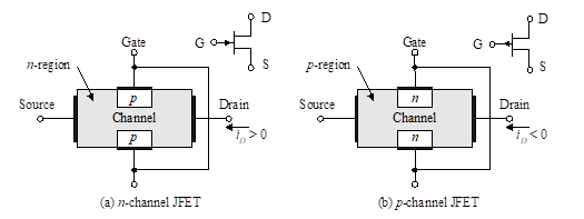
Figure 13-Physical Structure of JFET
VDD provides a drain-source voltage, vDS, that causes a drain current, iD, to flow from drain to source. Since the gate-source junction is reverse-biased, zero gate current results. The drain current, iD, which is equal to the source current, exists in the channel surrounded by the p-type gate. The gate-to-source voltage, vGS, which is equal to , creates a depletion region in the channel which reduces the channel width. This, in turn, increases the resistance between drain and source.
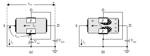
Figure 14 – n-channel JFET connected to external circuitry
We consider JFET operation with vGS = 0, as shown in Figure 14(b). The drain current, iD, through the n-channel from drain to source causes a voltage drop along the channel, with the higher potential at the drain-gate junction. This positive voltage at the drain-gate junction reverse-biases the pn junction and produces a depletion region, as shown by the dark shaded area in Figure 14(b). When we increase vDS, the drain current, iD, also increases, as shown in Figure 15.
This action results in a larger depletion region and an increased channel resistance between drain and source. As vDS is further increased, a point is reached where the depletion region cuts off the entire channel at the drain edge and the drain current reaches its saturation point. If we increase vDS beyond this point, iD remains relatively constant. The value of the saturated drain current with VGS = 0 is an important parameter. It is the drain-source saturation current, IDSS. We found it to be KVT2 for the depletion mode MOSFET. As can be seen from Figure 15, increasing vDS beyond this so-called channel pinch-off point (-VP, IDSS) causes a very slight increase in iD, and the iD-vDS characteristic curve becomes almost flat (i.e., iD remains relatively constant as vDS is further increased). Recall that VT (now designated VP) is negative for an n-channel device. Operation beyond the pinch-off point (in the saturation region) is obtained when the drain voltage, VDS, is greater than –VP (see Figure 15). As an example, let’s say VP = -4V, this means that the drain voltage, vDS, must be greater than or equal to –(-4V) in order for the JFET to remain in the saturation (normal operating) region.
This description indicates that the JFET is a depletion-type device. We expect its characteristics to be similar to those of the depletion MOSFETs. However there is an important exception: While it is possible to operate a depletion-type MOSFET in the enhancement mode (by applying a positive vGS if the device is n-channel) this is not practical in the JFET-type device. In practice, the maximum vGS is limited to approximately 0.3V since the pn-junction remains essentially cut-off with this small forward voltage.
Figure 15 –– iD versus vDS characteristic for n-channel JFET (VGS = 0V)
3.1 JFET Gate-To-Source Voltage Variation
In the previous section, we developed the iD-vDS characteristic curve with VGS = 0. In this section, we consider the complete iD-vDS characteristics for various values of vGS. Note that in the case of the BJT, the characteristic curves (iC-vCE) have iB as the parameter. The FET is a voltage-controlled device where vGS does the controlling. Figure 16 shows the iD-vDS characteristic curves for both the n-channel and p-channel JFET.
Figure 16-iD-vDS characteristic curves for JFET
As increases ![]() (vGS is more negative for an n-channel and more positive for a p-channel) the depletion region is formed and pinch-off is attained for lower values of iD. Hence for the n-channel JFET of Figure 16(a), the maximum iD reduces from IDSS as vGS is made more negative. If vGS is further decreased (more negative), a value of vGS is reached after which iD will be zero regardless of the value of vDS. This value of vGS is called VGS(OFF), or pinch-off voltage (Vp). The value of Vp is negative for an n-channel JFET and positive for a p-channel JFET. Vp can be compared to VT for the depletion mode MOSFET.
(vGS is more negative for an n-channel and more positive for a p-channel) the depletion region is formed and pinch-off is attained for lower values of iD. Hence for the n-channel JFET of Figure 16(a), the maximum iD reduces from IDSS as vGS is made more negative. If vGS is further decreased (more negative), a value of vGS is reached after which iD will be zero regardless of the value of vDS. This value of vGS is called VGS(OFF), or pinch-off voltage (Vp). The value of Vp is negative for an n-channel JFET and positive for a p-channel JFET. Vp can be compared to VT for the depletion mode MOSFET.
3.2 JFET Transfer Characteristics
The transfer characteristic is a plot of the drain current, iD, as a function of drain-to-source voltage, vDS, with vGS equal to a set of constant voltages (vGS = -3V, -2, -1V, 0V in Figure 16(a)). The transfer characteristic is nearly independent of the value of vDS since after the JFET reaches pinch-off, iD remains relatively constant for increasing values of vDS. This can be seen from the iD–vDS curves of Figure 16, where each curve becomes approximately flat for values of vDS>Vp.
In Figure 17, we show the transfer characteristics and the iD-vDS characteristics for an n-channel JFET. We plot these with a common iD axis to show how to obtain one from the other. The transfer characteristics can be obtained from an extension of the iD-vDS curves as shown by the dashed lines in Figure 17. The most useful method of determining the transfer characteristic in the saturation region is with the following relationship (the Shockley equation):
![]()
(16)
Hence, we need only know IDSS and Vp to determine the entire characteristic. Manufacturers’ data sheets often give these two parameters, so the transfer characteristic can be constructed. Vp in the manufacturer’s specification sheet is shown as VGS(OFF). Note that iD saturates, (i.e., becomes constant) as vDS exceeds the voltage necessary for the channel to pinch off. This can be expressed as an equation for vDS,sat for each curve, as follows:
![]()
(17)
As vGS becomes more negative, the pinch-off occurs at lower values of vDS and the saturation current becomes smaller. The useful region for linear operation is above pinch-off and below the breakdown voltage. In this region, iD is saturated and its value depends upon vGS, according to Equation (16) or the transfer characteristic.
Figure 17 – JFET transfer characteristics curves
The transfer and iD-vDS characteristic curves for the JFET, which are shown in Figure 17, differ from the corresponding curves for a BJT. The BJT curves can be represented as evenly spaced for uniform steps in base current because of the linear relationship between iC and iB. The JFET and MOSFET have no current analogous to a base current because the gate currents are zero. Therefore, we are forced to show the family of curves iD vs. vDS, and the relationships are very nonlinear.
The second difference relates to the size and shape of the ohmic region of the characteristic curves. Recall that in using BJTs, we avoid nonlinear operation by avoiding the lower 5% of values of vCE (i.e., the saturation region). We see that the width of the ohmic region for the JFET is a function of the gate-to-source voltage. The ohmic region is quite linear until the knee occurs close to pinch off. This region is called the ohmic region because when the transistor is used in this region, it behaves like an ohmic resistor whose value is determined by the value of vGS. As the magnitude of the gate-to-source voltage decreases, the width of the ohmic region increases. We also note from Figure 17 that the breakdown voltage is a function of the gate-to-source voltage. In fact, to obtain reasonably linear signal amplification, we must utilize only a relatively small segment of these curves – the area of linear operation is in the active region.
As vDS increases from zero, a break point occurs on each curve beyond which the drain current increases very little as vDS continues to increase. At this value of drain-to-source voltage, pinch-off occurs. The pinch-off values are labeled in Figure 17 and are connected with a dashed curve that separates the ohmic region from the active region. As vDS continues to increase beyond pinch-off, a point is reached where the voltage between drain and source becomes so large that avalanche breakdown occurs. (This phenomenon also occurs in diodes and in BJTs). At the breakdown point, iD increases sharply with a negligible increase in vDS. This breakdown occurs at the drain end of the gate-channel junction. Hence, when the drain-gate voltage, vDG, exceeds the breakdown voltage (BVGDS for the pn junction), avalanche occurs [for vGS = 0 V]. At this point, the iD-vDS characteristic exhibits the peculiar shape shown on the right part of Figure 17.
The region between the pinch-off voltage and avalanche breakdown is called the active region, amplifier operating region, saturation region, or pinch-off region. The ohmic region (before pinch-off) is usually called the triode region, but it is sometimes called the voltage-controlled region. The JFET is operated in the ohmic region both when a variable resistor is desired and in switching applications.
The breakdown voltage is a function of vGS as well as vDS. As the magnitude of the voltage between gate and source is increased (more negative for n-channel and more positive for p-channel), the breakdown voltage decreases (see Figure 17). With vGS = Vp, the drain current is zero (except for a small leakage current), and with vGS = 0, the drain current saturates at a value,
![]()
(18)
IDSS is the saturation drain-to-source current.
Between pinch-off and breakdown, the drain current is saturated and does not change appreciably as a function of vDS. After the JFET passes the pinch-off operating point, the value of iD can be obtained from the characteristic curves or from the equation
![]()
(19)
A more accurate version of this equation (taking into account the slight slope of the characteristic curves) is as follows:
![]()
(20)
λ is analogous to the λ for MOSFETs, and to 1/VA for BJTs. Since λ is small, we assume that ![]() . This justifies omitting the second factor in the equation and using the approximation for biasing and large signal analysis.
. This justifies omitting the second factor in the equation and using the approximation for biasing and large signal analysis.
The saturation drain-to-source current, IDSS, is a function of temperature. The effects of temperature upon Vp are not large. However, IDSS decreases as temperature increases, the decrease being as much as 25% for a 100o increase in temperature. Even larger variations occur in Vp and IDSS because of slight variations in the manufacturing process. This can be seen by viewing the Appendix for the 2N3822 where the maximum IDSS is 10 mA and the minimum is 2 mA.
The currents and voltages in this section are presented for an n-channel JFET. The values for a p-channel JFET are the reverse of those given for the n-channel.
3.3 JFET Small-Signal ac Model
A JFET small-signal model can be derived following the same procedures used for the MOSFET. The model is based on the relationship of Equation (20). If we consider only the ac component of the voltages and currents, we have
![]()
(21)
The parameters in Equation (21) are given by the partial derivatives,
![]()
(22)
The resulting model is shown in Figure 18. Note that the model is identical to the MOSFET model derived previously, except that the values of gm and ro are calculated using different formulae. Actually the formulas are identical if Vp is substituted for VT.
Figure 18 – JFET small signal ac model
To design a JFET amplifier, the Q-point for the dc bias current can be determined either graphically, or by using circuit analysis assuming pinch-off mode for the transistor. The dc bias current at the Q-point should lie between 30% and 70% of IDSS. This locates the Q-point in the most linear region of the characteristic curves.
The relationship between iD and vGS can be plotted on a dimensionless graph (i.e., a normalized curve) as shown in Figure 20.
The vertical axis of this graph is iD/IDSS and the horizontal axis is vGS/Vp. The slope of the curve is gm.
A reasonable procedure for locating the quiescent value near the center of the linear operating region is to select and . Note from Figure 6.20 that this is near the midpoint of the curve. Next, we select . This gives a wide range of values for vds that keep the transistor in the pinch-off mode.
Figure 20 –iD/IDSS versus vGS/Vp
We can find the transconductance at the Q-point either from the slope of the curve of Figure 20 or by using Equation (22). If we use this procedure, the transconductance parameter is given by,
![]()
(23)
Remember that this value of gm depends on the assumption that ID is set at one-half IDSS and VGS . 0.3Vp. These values usually represent a good starting point for setting the quiescent values for the JFET.