
1. Differential Amplifiers
 CURRENT – 1. Differential Amplifiers
 PREVIOUS- Practical Operational Amplifiers- Introduction
Differential Amplifiers
Most operational amplifiers are comprised of a series of transistors, resistors, and capacitors forming a complete system on a single chip. The amplifiers available today are reliable, small in size, and consume very little power.
The input stage of most op-amps is a Differential Amplifier as shown in its simplest form in Figure 1.
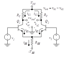
Figure 1 – Differential amplifier
The differential amplifier is composed of two emitter-coupled common-emitter dc amplifiers. It has two inputs, v1 and v2, and three outputs, vo1, vo2 and vout. The third output, vout, is the difference between vo1 and vo2.
1.1 dc Transfer Characteristics
The differential amplifier does not operate linearly with large signal inputs. In order to simplify the analysis we assume that RE is large, that the base resistance of each transistor is negligible and that the output resistance of each transistor is large. Note that we use REE rather than RE in the differential amplifier since the resistor used here is large and may be the equivalent resistance of a current source. The large value of REE keeps the emitter resistor voltage drop nearly constant.
We now solve this circuit for the output voltage. We begin by writing a KVL equation around the base junction loop for the circuit of Figure 1.
(1)
(2)
We need to find expressions for the collector currents, iC1 and iC2. The base-emitter voltages are given by the equation,
In Equation (2) Io1 and Io2 are the reverse saturation currents for Q1 and Q2 respectively. The transistors are assumed to be identical. Combining Equations (1) and (2) yields
(3)
Solving Equation (3) for the current ratio, we find,
(4)
We can assume iC1 is approximately equal to iE1 and iC2 is approximately equal to iE2. Therefore
(5)
Combining Equations (4) and (5) , we have
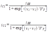
(6)
Note that
(7)
An important observation can be made by viewing Equation (6) . If v1 – v2 becomes greater than several hundred millivolts, the collector current in transistor 2 becomes small and the transistor is essentially cut off. The collector current in transistor 1 is approximately equal to iEE, and this transistor is saturated. The collector currents, and therefore the output voltage vout, become independent of the difference between the two input voltages.
Linear amplification occurs only for input voltage differences less than approximately 100 mV. In order to increase the linear range of the input voltage, small emitter resistors can be added.
1.2 Common-Mode and Differential-Mode Gains
The differential amplifier is intended to respond only to the difference between the two input voltages, v1 and v2. However, in a practical op-amp the output depends to some degree on the sum of these inputs. For example, if both inputs are equal, the output voltage should ideally be zero, but in a practical amplifier it is not. We label the case when the circuit responds to the difference as the differential mode. If the two inputs are made equal, we say the circuit is in its common mode. Ideally we would expect the circuit to produce an output only in the differential mode.
Any two input voltages, v1 and v2, can be resolved into a common and a differential part. We define two new input voltages as follows:

(8)
The voltage, vdi, is the differential-mode input voltage and it is simply the difference between the two input voltages. The voltage, vci, is the common-mode input voltage, and it is the average of the two input voltages. The original input voltages can be expressed in terms of these new quantities as follows:
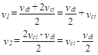
(9)
If we set the two input voltages equal, we have
(10)
Since the two inputs are equal, the emitter-base junction voltages are equal (if the transistors are identical). Thus, the collector currents must also be identical.
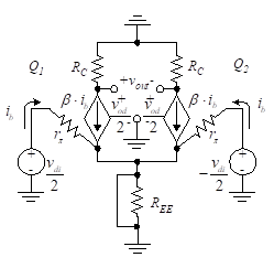
Figure 2(a) Differential-mode amplifier equivalent circuit
We now view the equivalent circuit for the differential-mode input voltage as shown in Figure 2(a). Note that as the current in the Q1 circuit increases, the current in the Q2 circuit decreases at the same rate and amplitude. This is true since the input to Q2 is equal to that of Q1 but 180o out of phase. Thus the voltage change across REE is zero. Since the ac signal voltage across REE is zero, it can be replaced by a short circuit in the ac equivalent circuit. Note that placing voltages at each transistor base which are equal in amplitude but 180o out of phase is equivalent to placing a voltage between the two transistor bases of twice the amplitude. The voltages at vo1 and vo2 are of equal amplitude but opposite phase and the differential-mode gain is
(11)
This differential-mode gain is defined at a single-ended output since it is taken between one collector and ground. If the output is taken between vo1 and vo2, the differential-mode gain is termed a double-ended output and is given by
(12)
A similar analysis can be applied to the common-mode equivalent circuit in Figure 2(b).
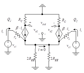
Figure 2(b) Common-mode amplifier equivalent circuit
If we divide the resistor REE into two parallel resistors each having double the original resistance, we can find the output by analyzing only half of the circuit. Since the transistors are identical and the common-mode input voltages are equal and in-phase, the voltages across the 2REE resistors are the same. Thus, the current between the two parallel resistors shown for is zero and we need only look at one side of the circuit. The common-mode voltage gain is then
(13)
Equation (13) assumes REE is large and re<<REE.
We find the double-ended output voltage in terms of the common-mode and differential-mode gain as follows:
(14)
It is desirable for the differential-mode gain to be much larger than the common-mode gain so that the amplifier reacts primarily to the difference between the input voltages. The common-mode rejection ratio, CMRR, is defined as the ratio of the differential-mode gain to the common-mode gain. It is usually expressed in dB.
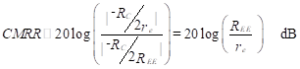
(15)
We now determine the input resistance of the amplifier in both the differential mode and the common mode. For the differential mode, we look into the amplifier at the base of both transistors. This results in a complete circuit through the emitter of both transistors, and the input resistance is
(16)
Now for the common-mode input, we look into the amplifier in Figure 2(b). Thus, the input resistance is
(17)
These results indicate that the input resistance of the common mode is much higher than that of the differential mode.
Our differential amplifier analysis is based upon BJTs as the transistor building blocks. FETs can also be used in differential amplifiers with the resulting advantages of reduced input bias current and nearly infinite input impedance. The analysis of the differential amplifier using FETs is accomplished in the same way as that of BJT analysis.
Differential amplifiers need matched transistors to insure that the circuit operates correctly. If the differential amplifier is on an integrated circuit, this additional requirement is less of a problem since the two transistors are fabricated at the same time using the same material.
1.3 Differential Amplifier with Constant Current Source
It is desirable to make REE as large as possible in order to reduce the common-mode output. Equation shows that to make the CMRR large we must make REE large. Since large resistances are hard to fabricate on IC chips, we seek an alternate approach. This is accomplished by replacing REE with a dc current source. An ideal current source has infinite impedance, so we investigate the possibility of replacing REE with such a current source. Figure 9.3 illustrates a differential amplifier where the resistor, REE, is replaced with a constant-current source.
(18)
The closer the source is to the ideal constant-current source, the higher the common-mode rejection ratio. We illustrate a diode-compensated fixed-bias current source. The compensation makes the operation of the circuit less dependent on temperature variations. Diode D1 and transistor Q3 are selected so that they have nearly identical characteristics over the range of operating temperatures.
In order to analyze the circuit of Figure 3(a) and find the CMRR, we need to determine the equivalent resistance, RTH (the Thevenin equivalent of the constant current source circuit). The equivalent resistance is given by [see Figure 3(b)]
Writing a KCL equation at node 1, we have
(19)
where ro is the internal resistance of the transistor at the specified operating point. It is given by
(20)
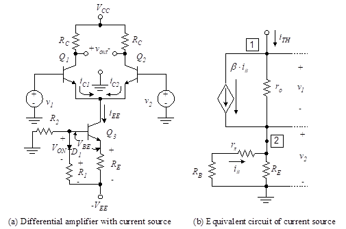
Figure 3 – Differential amplifier with constant-current source
A KCL equation at node 2 yields
(21)
where
(22)
Substituting v1 and v2 into the equation at node 2, we have
(23)
Finally, the Thevenin resistance is given by substituting Equations (22) and (23) into Equation (18) .
(24)
We will now make a series of assumptions to greatly simplify this expression. To maintain bias stability, we use the guideline that
(25)
Substituting this value of RB in Equation (24) and dividing by β, we have
(26)
We can simplify this expression by noting
(27)
We then have
(28)
Since the second term in this equation is much greater than the first, so we can ignore RE to obtain
(29)
This equation can be further simplified if the following condition exists:
(30)
In that case, we have the simple result
(31)
Hence, if all of the approximations are valid, RTH is independent of β and its value is quite large.
1.4 Differential Amplifier with Single-Ended Input and Output
Figure 4 shows a differential amplifier where the second input, v2, is set equal to zero and the output is taken as vo1.
We use a constant current source in place of REE, as discussed in the previous section. This is known as a single-ended input and output amplifier with phase reversal. The amplifier is analyzed by setting v2 = 0 in the earlier equations. The differential input is then simply
(32)
so the output is
(33)
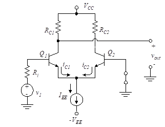
Figure 4 – Single-ended input with phase reversal
The minus sign indicates that this amplifier exhibits an 180o phase shift between the output and input. A typical sinusoidal input and output are illustrated in Figure 5.
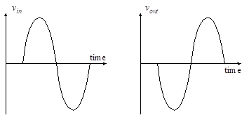
Figure 5 – Sinusoidal input and output
If an output signal is to be referenced to ground but a phase reversal is not desired, the output can be taken from transistor Q2.
Example 1 – Differential Amplifier (Analysis)
Find the differential voltage gain, the common-mode voltage gain, and the CMRR for the circuit shown in Figure 1. Assume that Ri = 0, RC = 5 kΩ, VEE = 15 V, VBE = 0.7 V, VT = 26 mV, and REE = 25 kΩ. Let v2 = 0 and take the output from vo2.
Solution: The current through REE is found at the quiescent condition. Since the base of Q2 is grounded, the emitter voltage is VBE = 0.7 V, and
![]()
The quiescent current in each transistor is one-half of this amount.
![]()
Since
![]()
the differential voltage gain in each transistor is
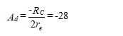
The common-mode voltage gain is
![]()
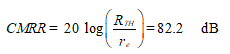
The common-mode rejection ratio is then given by
![]()
APPLICATION
Also, you can carry out these calculations with TINA or TINACloud circuit simulators, using their Interpreter tool by clicking the link below.
1- Differential Amplifier Circuit Simulation
Example 2
For the differential amplifier described in Example 1, design a temperature-compensated fixed-bias current source (Figure 3) to replace REE and determine the new CMRR for the differential amplifier, with ro = 105 kΩ, VBE = 0.7 V, and β = 100. Assume R1 = R2.
Solution: We place the transistor operating point in the middle of the dc load line.
![]()
Then, referring to the current source of Figure 3(a),
![]()
For bias stability,
![]()
Then
![]()
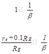
Since 0.1RE>>re (i.e., 1.25 kΩ >> 26/0.57 Ω), then from Equation (31) we have
![]()
The CMRR is given by
APPLICATION
Also, you can carry out these calculations with TINA or TINACloud circuit simulators, using their Interpreter tool by clicking the link below.
2- Differential Amplifier Circuit Simulation
Example 3
Design a circuit to attain the conditions as specified in Figure 6 for maximum output voltage swing. The five transistors, Q1 to Q5, each have β = 100 while Q6 has a β of 200. VBE is 0.6 V for all transistors, VT = 26 mV, and VA = 80 V. Assume all transistors are identical.
Determine,
(a) RC, R1, and CMRR.
(b) Common-mode output voltage.
(c) Differential-mode output voltage.
(d) Differential-mode input voltage vdi for maximum output.
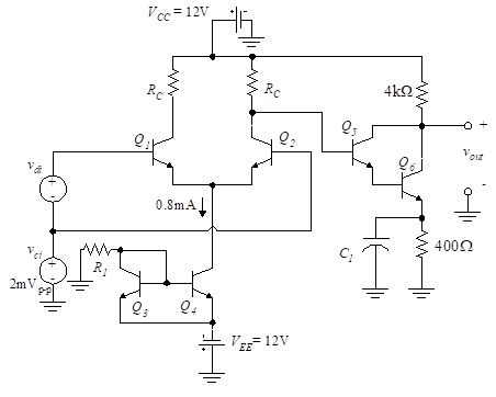
Figure 6 – Differential amplifier for Example 3
Solution: We shall treat the circuit in three sections:
- 1. Darlington amplifier.
- 2. Differential amplifier
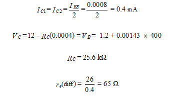
- 3. Simple current source
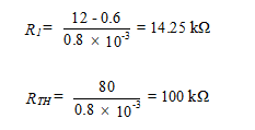
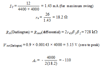
Now for the total system, we have
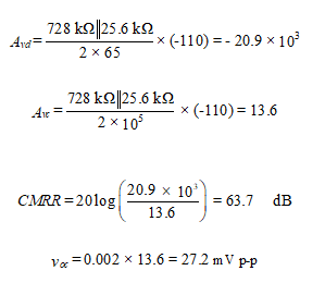
The differential input vdi necessary to produce maximum undistorted output voltage swing is
![]()
APPLICATION
Also, you can carry out these calculations with TINA or TINACloud circuit simulators, using their Interpreter tool by clicking the link below.
3- Differential Amplifier Circuit Simulation