
4. Input resistance of Op-amp circuits
 CURRENT – 4. Input resistance of Op-amp circuits
 PREVIOUS- 3. The non-inverting amplifier
Input resistance of Op-amp circuits
The input resistance of the ideal op-amp is infinite. However, the input resistance to a circuit composed of an ideal op-amp connected to external components is not infinite. It depends on the form of the external circuit.
We first consider the inverting op-amp. The equivalent circuit for the inverting op-amp of Figure (3) “The inverting op-amp” is shown in Figure 10(a).
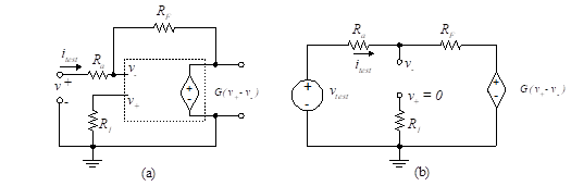
Figure 10- Input resistance, inverting amplifier
Figure 10 (b) shows the same circuit rearranged for simplicity of analysis. Note that we have attached a “test” voltage source to the input in order to calculate the equivalent resistance. Since the circuit contains a dependent voltage source, we can’t find the input resistance by simply combining resistors. Instead, we find the input resistance by replacing the input signal source and its associated resistance with a test source of specified voltage, vtest, and then calculate the current delivered by the test source to the circuit, itest. Alternatively, we could use a current test source, itest, and solve for the voltage delivered to the circuit, vtest. Using either technique, we can calculate the resistance from Ohm’s law.
The loop equation is given by,
(26)
The equivalent input resistance is then
(27)
As the loop gain, G, approaches infinity, the first term in Equation (27) approaches zero and the input resistance approaches Ra. Thus, the input resistance seen by the source is equal to the value of the external resistance, Ra. This verifies the virtual ground property since the result indicates that the inverting input is equivalent to a ground.
We now consider the inverting amplifier with two inputs.
This is shown in Figure (11).
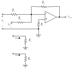
Figure 11- Two-input inverting amplifier
It is a special case of the circuit of Figure (4) “Op-amp circuit” shown previously.
Since the voltage at the inverting input to the op-amp is zero (virtual ground), the input resistance seen by va is Ra, and that seen by vb is Rb. The “grounded” inverting input also serves to isolate the two inputs from each other. That is, a variation in va does not affect the input vb, and vice versa.
The input resistance for the non-inverting amplifier can be determined by referring to the circuit configuration of Figure (5) “Non-inverting amplifier” . See the equivalent circuit in Figure 12(a).
No current passes through R1 since the v+ input to the op-amp has infinite resistance. As a result, Rin to a non-inverting terminal is infinity. If a design needs a large input resistance, we often use a single-input non-inverting op-amp. Such a configuration is called a non-inverting buffer if it has a voltage gain of unity.
Therefore the situation changes when we go to a multiple input non-inverting op-amp, as shown in Figure 12(b). The equivalent circuit is shown in Figure 12(c). We are assuming that the resistance associated with each source, (r1, r2 and r3) is zero ohms. When applying the test source to calculate the input resistance for multiple-input circuits, we use superposition. We therefore apply the test source at each input separately while disabling the other inputs (short circuits for voltage sources and open circuits for current sources in accordance with the principle of Superposition). The various input resistances are then
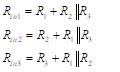
(28)
APPLICATIONS
Analyze the following circuits online using the TINACloud circuit simulator by clicking the links below.
1- Input Resistance of an Inverting Amplifier Circuit Simulation
2- Input Resistance of a two-input Inverting Amplifier Circuit Simulation
This concept can easily be extended to n inputs.
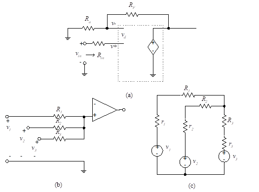
Figure 12- Input resistance of a non-inverting amplifier