
5. MOSFET Integrated Circuits
 CURRENT – 5. MOSFET Integrated Circuits
 PREVIOUS- 4. FET Amplifier Configurations and Biasing
MOSFET Integrated Circuits
When MOSFET transistors are fabricated as part of an integrated circuit, practical considerations require two major changes in circuit configurations. First, the large coupling and bypass capacitors used in discrete amplifiers cannot practically be fabricated in integrated circuits because of the small size. We get around this shortcoming by fabricating direct-coupled amplifiers.
The second major change is that we cannot easily fabricate the resistors used as part of the bias circuitry. Instead, we use active loads and current sources comprised of MOS transistors.
Integrated circuits use both NMOS and PMOS circuitry. CMOS is more common in digital circuitry, while NMOS is typically used for higher density ICs (i.e., more functions per chip).
Simulating active loads takes advantage of the slope of the MOS characteristic curves. Figure 23 shows two types of active loads. In Figure 23(a), we show an NMOS enhancement load, while 23(b) shows an NMOS depletion load. Also shown in the figure are the relevant characteristic curves.
Figure 23 – Active loads
For the NMOS enhancement load, the relationship between voltage and current is given by
![]()
(29)
The equivalent resistance of this configuration is 1/gm, where the value of the transconductance is that which applies at the bias point.
The NMOS depletion load has an equivalent resistance which is determined by the slope of the characteristic given by the following equation
![]()
(30)
5.1 Biasing of MOSFET Integrated Circuits
Now that we have two techniques to simulate active loads, we can address the biasing issue. We use the active load in place of the load resistance in any of the circuit configurations. To show the technique for analyzing these, let us consider the NMOS amplifier using an enhancement load, as shown in Figure 24.
The transistor labeled Q2 replaces RD of our earlier circuitry. To determine the quiescent operating point, we use the same techniques as we did in Section 4, “FET Amplifier configurations and biasing” only substituting the enhancement load graphical characteristic for the resistor load line. That is, we need to find the simultaneous solution of the FET transistor characteristics with the equation for the load line. We can do this graphically as shown in Figure 25.
The parametric curves are the characteristic curves for the amplifying transistor, Q1. The voltage vs. current characteristic of the active load, Q2 are those of Figure 23. The output voltage, vout, is the difference between VDD and the voltage across the active load. The current in the active load is the same as the drain current in the amplifying transistor. We therefore construct the load line by taking the shifted mirror image of the characteristic of Figure 23. The operating point is the intersection of this curve with the appropriate transistor characteristic curve. We need to find the gate-to-source voltage to know which transistor curve to choose. As we will see next, the input bias voltage is often replaced by an active current source.
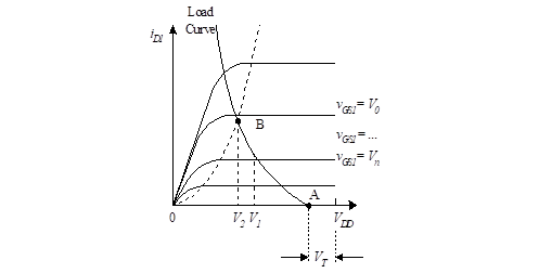
Figure 25 – Graphical solution for the Q-point
Now that we know how to simulate an active load, we turn our attention to the generation of a reference current to be used as part of the input bias circuitry. These current sources are used in much the same way that we used them for BJT amplifier biasing.
Figure 26 – Current mirror
We analyze the MOSFET current mirror. A current mirror is shown in Figure 26. The two transistors are assumed to be perfectly matched. The output current is the drain current of Q2, and a reference current drives Q1. If the transistors are perfectly matched, the output current will exactly equal the reference current. This is true since the transistors are connected in parallel. Just as was the case with the BJT current mirror, the reference current can be generated by applying a reference voltage across a reference resistance, as shown in Figure 26(b).
Putting the various subcircuits together (i.e., the active load and the reference current) results in the CMOS amplifier of Figure 27.
The gain of this amplifier is given by
![]()
(31)
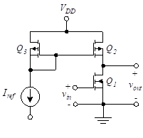
Figure 27 – CMOS amplifier
5.2 Body Effect
Our discussion of Section “2. Metal-oxide semiconductor FET (MOSFET)” referred to the substrate (or body) of the MOSFET. This substrate plays an important role in establishing the channel. In the operation of discrete MOSFETs, the body is often connected to the power source. In such cases, the substrate has no direct effect on the operation of the device, and the curves developed earlier in this chapter apply.
The situation changes when MOSFETs are fabricated as part of integrated circuits. In such cases, the substrate of each individual transistor is not isolated from other substrates. Indeed, a substrate is often shared among all of the MOSFETs on a chip. In a PMOS IC, the shared substrate would be connected to the most positive source terminal, while in NMOS it is connected to ground (or to a negative supply if present). This establishes a reverse bias between the source and the body of each transistor. The effect of this reverse bias is to change the operating characteristics. For example, in an n-channel device, it effectively raises the threshold (VT). The amount by which the threshold changes depends on physical parameters and the device construction. For NMOS, this change can be approximated by
![]()
(32)
In Equation (32), γ is a device parameter which varies between about 0.3 and 1 (V-1/2). VSB is the source-to-body voltage, and is the Fermi potential. This is a property of the material, and a typical value is 0.3 V for silicon.