
6. Design of Op-amp Circuits
 CURRENT – 6. Design of Op-amp Circuits
 PREVIOUS- 5. Combined inverting and non-inverting inputs
Design of op-amp circuits
Once the configuration of an op-amp system is given, we can analyze that system to determine the output in terms of the inputs. We perform this analysis using the procedure discussed earlier (in this chapter).
If you now wish to design a circuit that combines both inverting and non-inverting inputs, the problem is more complex. In a design problem, a desired linear equation is given, and the op-amp circuit must be designed. The desired output of the operational amplifier summer can be expressed as a linear combination of inputs,
(30)
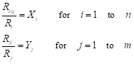
where X1, X2 …Xn are the desired gains at the non-inverting inputs and Ya, Yb …Ym are the desired gains at the inverting inputs. Equation (30) is implemented with the circuit of Figure (14).
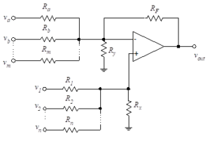
Figure 14- Multiple input summer
This circuit is a slightly modified version of the circuit of Figure (13) (Inverting and non-inverting inputs).
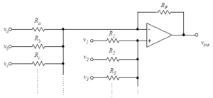
Figure 13- Inverting and non-inverting inputs
The only change we have made is to include resistors between the op-amp inputs and ground. The ground can be viewed as an additional input of zero volts connected through the corresponding resistor (Ry for the inverting input and Rx for the non-inverting input). The addition of these resistors gives us flexibility in meeting any requirements beyond those of Equation (30). For example, the input resistances might be specified. Either or both of these additional resistors can be removed by letting their values go to infinity.
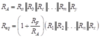
Equation (29) from the previous section shows that the values of the resistors, Ra, Rb, …Rm and R1, R2, …Rn are inversely proportional to the desired gains associated with the respective input voltages. In other words, if a large gain is desired at a particular input terminal, then the resistance at that terminal is small.
When the open loop gain of the operational amplifier, G, is large, the output voltage may be written in terms of the resistors connected to the operational amplifier as in Equation (29) . Equation (31) repeats this expression with slight simplification and with addition of the resistors to ground.
(31)
We define two equivalent resistances as follows:
(32)
APPLICATION
Analyze the following circuit using TINACloud to determine Vout in terms of the input voltages by clicking the link below.
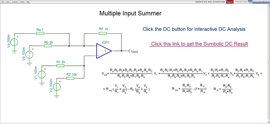
Multiple Input Summer Circuit Simulation by TINACloud
Multiple Input Summer Circuit Simulation by TINACloud
We see that the output voltage is a linear combination of inputs where each input is divided by its associated resistance and multiplied by another resistance. The multiplying resistance is RF for inverting inputs and Req for non-inverting inputs.
The number of unknowns in this problem is n+m+3 (i.e. the unknown resistor values). We therefore need to develop n+m+3 equations in order to solve for these unknowns. We can formulate n+m of these equations by matching the given coefficients in Equation (30) . That is, we simply develop the system of equations from Equations (30), (31) and (32)as follows:
(33)
Since we have three more unknowns, we have the flexibility to satisfy three more constraints. Typical additional constraints include input resistance considerations and having reasonable values for the resistors (e.g., You would not want to have to use a precision resistor for R1 equal to 10-4 ohms!).
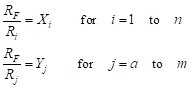
Although not required for design using ideal op-amps, we will use a design constraint that is important for non-ideal op-amps. For the non-inverting op-amp, the Thevenin resistance looking back from the inverting input is usually made equal to that looking back from the non-inverting input. For the configuration shown in Figure (14), this constraint can be expressed as follows:
(34)
The last equality results from the definition of RA from Equation (32). Substituting this result into Equation (31) yields the constraint,
(35)
(36)
Substituting this result into Equation (33) yields the simple set of equations,
(37)
The combinations of Equation (34) and Equation (37) give us the necessary information to design the circuit. We select a value of RF and then solve for the various input resistors using Equation (37) . If the values of the resistors are not in a practical range, we go back and change the value of the feedback resistor. Once we solve for the input resistors, we then use Equation (34) to force the resistances to be equal looking back from the two op-amp inputs. We select values of Rx and Ry to force this equality. While Equations (34) and (37) contain the essential information for the design, one important consideration is whether or not to include the resistors between the op-amp inputs and ground (Rx and Ry). The solution may require iterations to obtain meaningful values (i.e. you may perform the solution one time and come up with negative resistance values). For this reason, we present a numerical procedure which simplifies the amount of calculations[1]
Equation (34) can be rewritten as follows:
(38)
Substituting Equation (37) into Equation (38) we obtain,
(39)
Recall that our goal is to solve for the resistors values in terms of Xi and Yj. Let us define summation terms as follows:

(40)
We can then rewrite Equation (39) as follows:
(41)
This is a starting point for our design procedure. Recall that Rx and Ry are the resistors between ground and the non-inverting and inverting inputs, respectively. The feedback resistor is denoted RF and a new term, Z, is defined as
(42)
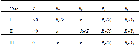
Table (1)-Summing Amplifier Design
We can eliminate either or both of the resistors, Rx and Ry, from the circuit of Figure (14). That is, either or both of these resistors can be set to infinity (i.e., open-circuited). This yields three design possibilities. Depending on the desired multiplying factors relating output to input, one of these cases will yield the appropriate design. The results are summarized in Table (1).
Circuit design with TINA and TINACloud
There are several tools available in TINA and TINACloud for operational amplifier and circuit design.
Optimization
TINA‘s Optimization Mode unknown circuit parameters can be determined automatically so that the network can produce a predefined target output value, minimum or maximum. Optimization is useful not only in circuit design, but in teaching, to construct examples and problems. Note that this tool works not only for ideal op-amps and linear circuit, but for any nonlinear circuit with real nonlinear and other device models.
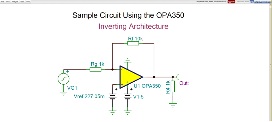
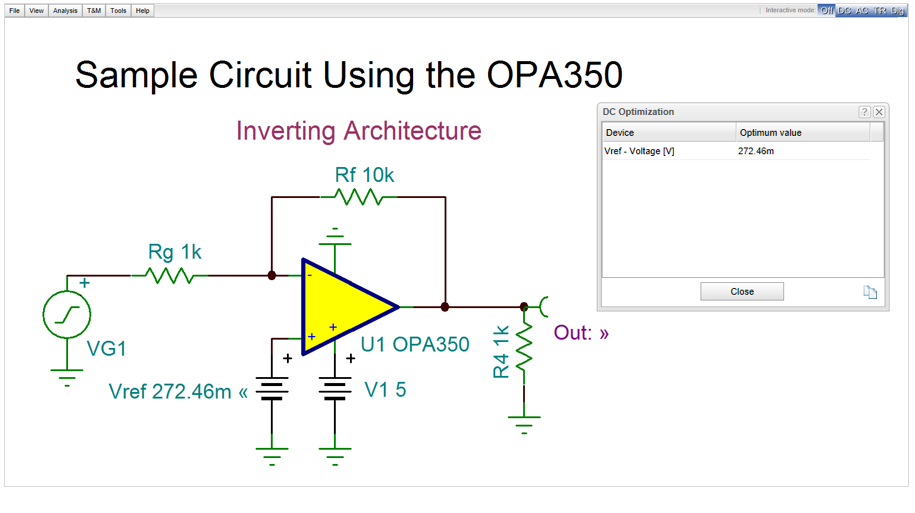
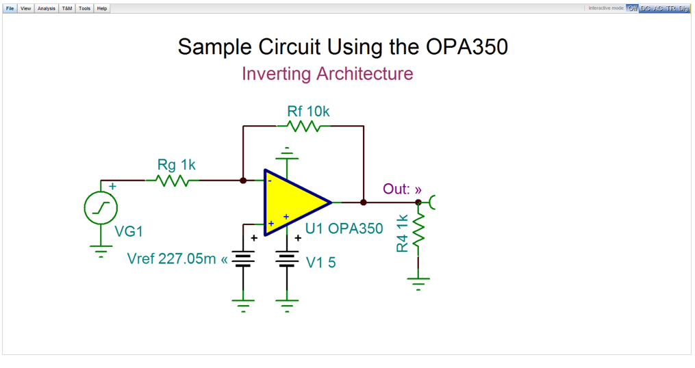
Consider the inverting amplifier circuit with a real operational amplifier OPA350.
By the default setting of this circuit the output voltage of the circuit is 2.5
You can easily check this by pressing the DC button in TINACloud.
APPLICATION
Analyze the following circuit using the TINACloud online circuit simulator to determine Vout in terms of the input voltages by clicking the link below.
OPA350 Circuit Simulation with TINACloud
OPA350 Circuit Simulation with TINACloud
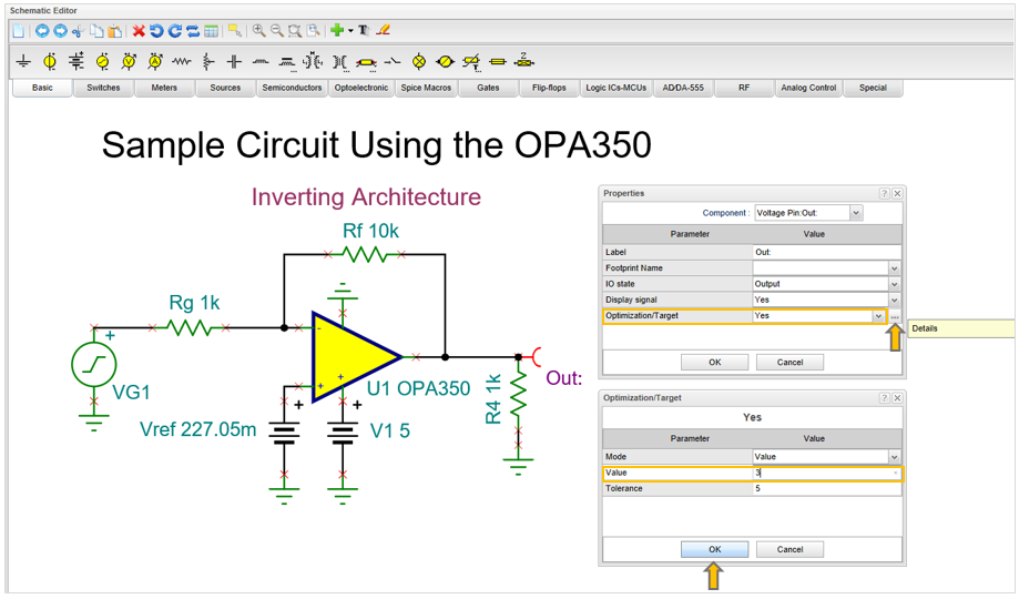
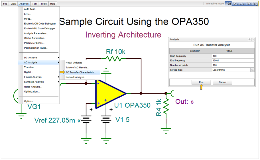
If order to prepare this we should select the target Out=3V and circuit parameter to be determined (Optimization Object) Vref. For this object we should also define a region which helps the search but also represents the constraints.
To select and set the Optimization target in TINACloud click Vout Voltage pin and set the Optimization Target to Yes
Next click the … button in the same line and set the Value to 3.
Press OK in each dialog to finish the settings.
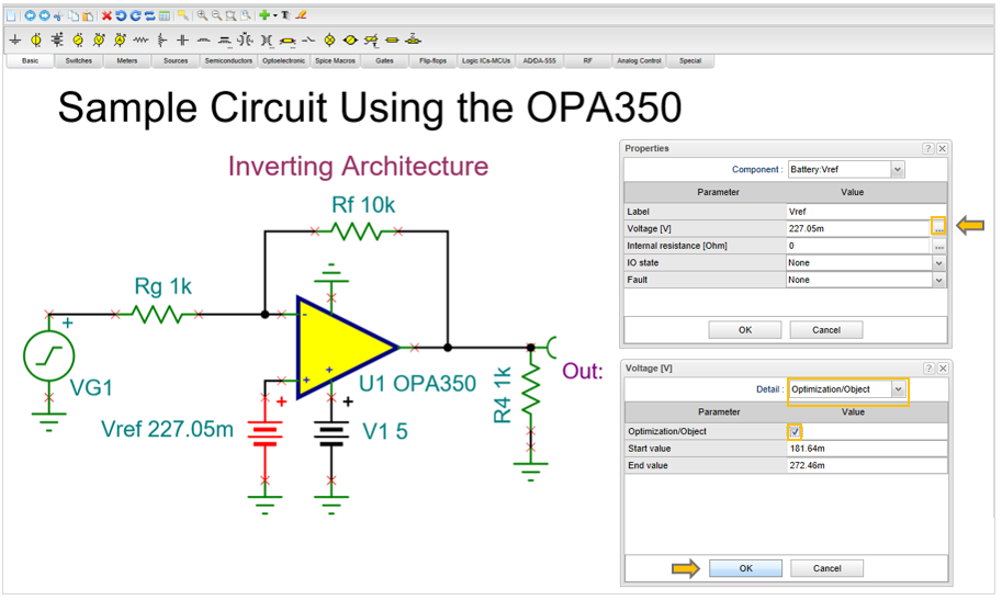
Now let’s select and set the Vref Optimization Object.
Click Vref then the … button in the same line
Select Optimization Object in the list on he top and set the Optimization/Object checkbox.
Press OK in both dialogs.
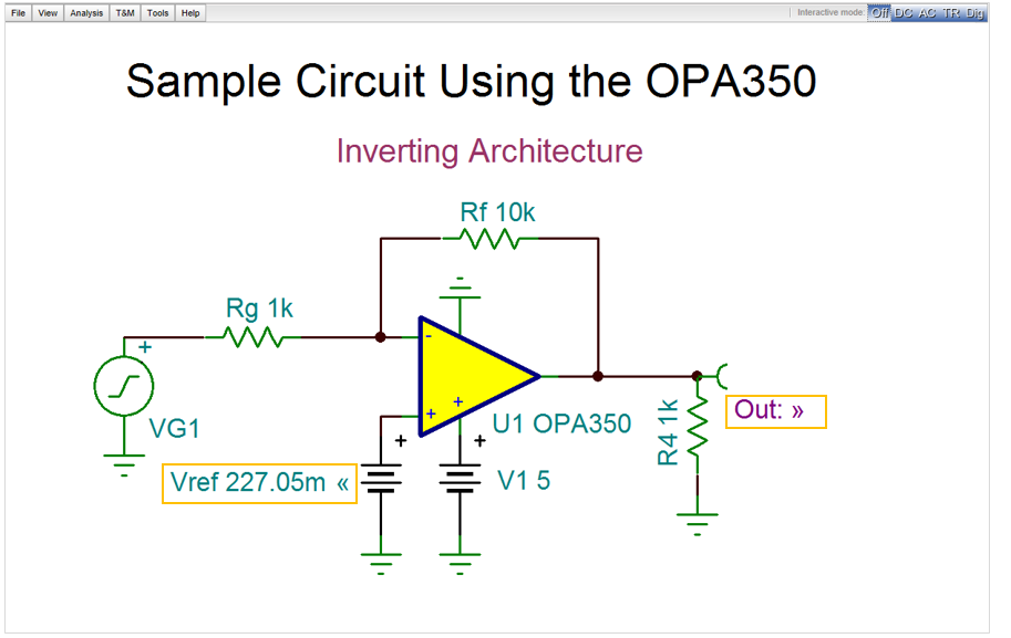
If the Optimization settings were successfully you will see a >> sign at Out and a << sign at Vref as shown below.
Now select Optimization from the Analysis menu and press RUN in the Optimization dialog box.
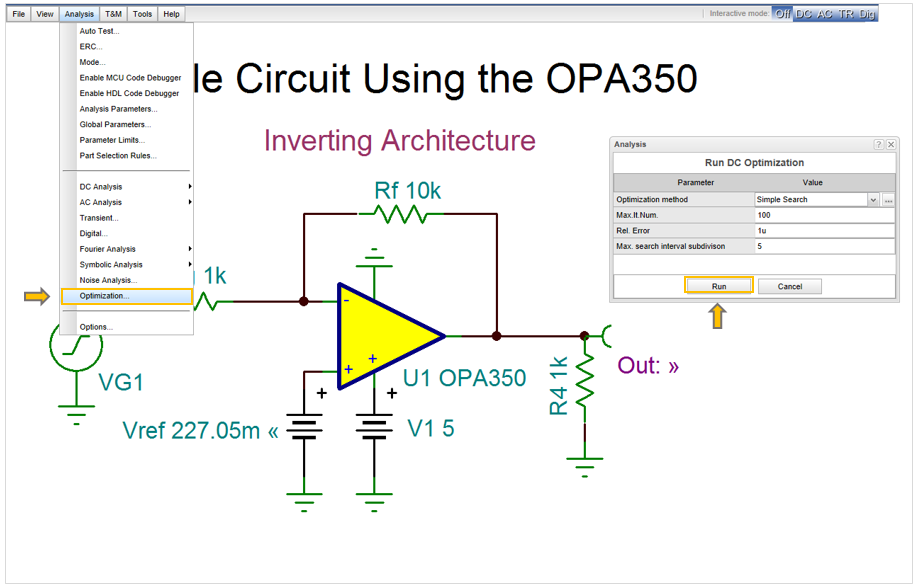
After completing the Optimization the found Vref, the Optimum Value, will be shown in the DC Optimization dialog
You can study the settings and run the Optimization online and check by Circuit Simulation using the link below.
Run Optimization from the Analysis menu then press the DC button so see the result in the Optimized circuit (3V)
Online Optimization and Circuit Simulation with TINACloud
Note that at this time in TINACloud only a simple DC optimization is included. More optimizations features are included in the offline version of TINA.
AC Optimization
Using the offline version of TINA you can optimize and redesign AC circuits as well.
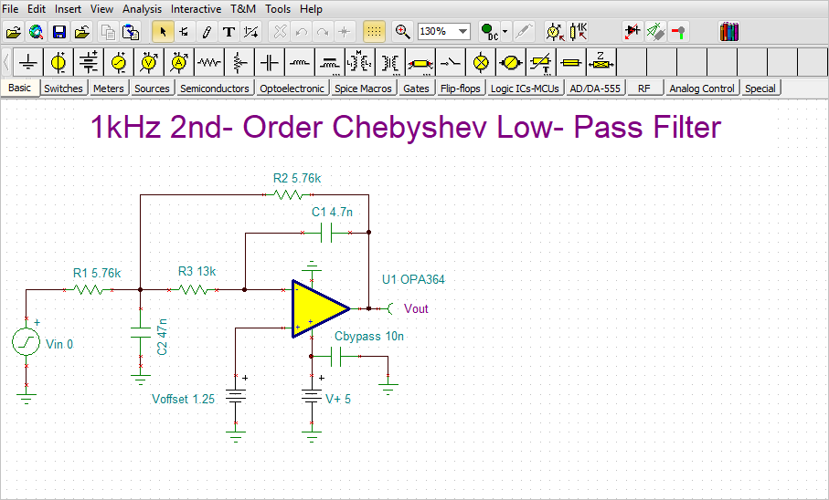
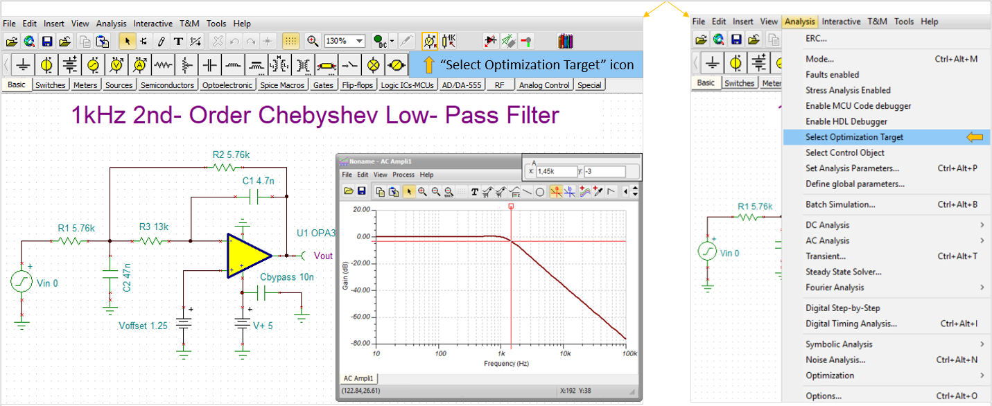
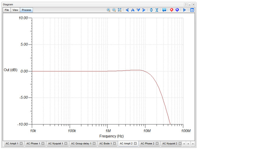
Open the MFB 2nd Order Chebyshev LPF.TSC low-pass circuit, from the Examples\Texas Instruments\Filters_FilterPro folder of TINA, shown below.
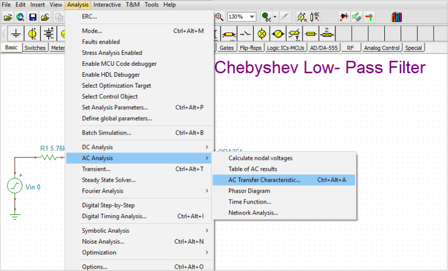
Run AC Analysis/AC Transfer Characteristic.
The following diagram will appear:
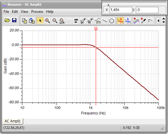
The circuit has unity (0dB) Gain and 1.45kHz Cutoff frequency.
Now let’s redesign the circuit using AC Optimization and set the low frequency Gain to 6dB and the Cutoff frequency to 900Hz.
Note that normally the optimization tool applicable for changes only. In case of filters you may want to use rather a filter design tool. We will deal with that topic later.
Now using Optimization the Gain and the Cutoff frequency are the Optimization targets.
Click the “Select Optimization Target” icon on the toolbar or on the Analysis menu “Select Optimization Target”
The cursor will change into the icon: ![]() . Click the Vout Voltage pin with the new cursor symbol.
. Click the Vout Voltage pin with the new cursor symbol.
The following dialog will appear:
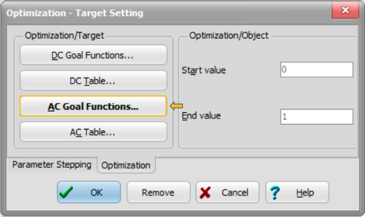
Click the AC Goal Functions Buttons. The following dialog will appear:
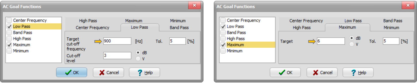
Check the Low Pass checkbox and set the Target cut-off frequency to 900. Now check the Maximum checkbox and set the Target to 6.
Next select the circuit parameters which you want to change to reach the Optimization targets.
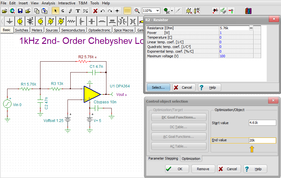
Click the ![]() symbol or the Select Control Object line on the Analysis menu.
symbol or the Select Control Object line on the Analysis menu.
The cursor will change to the symbol above. Click the C1 capacitor with this new cursor. The following dialog will appear:
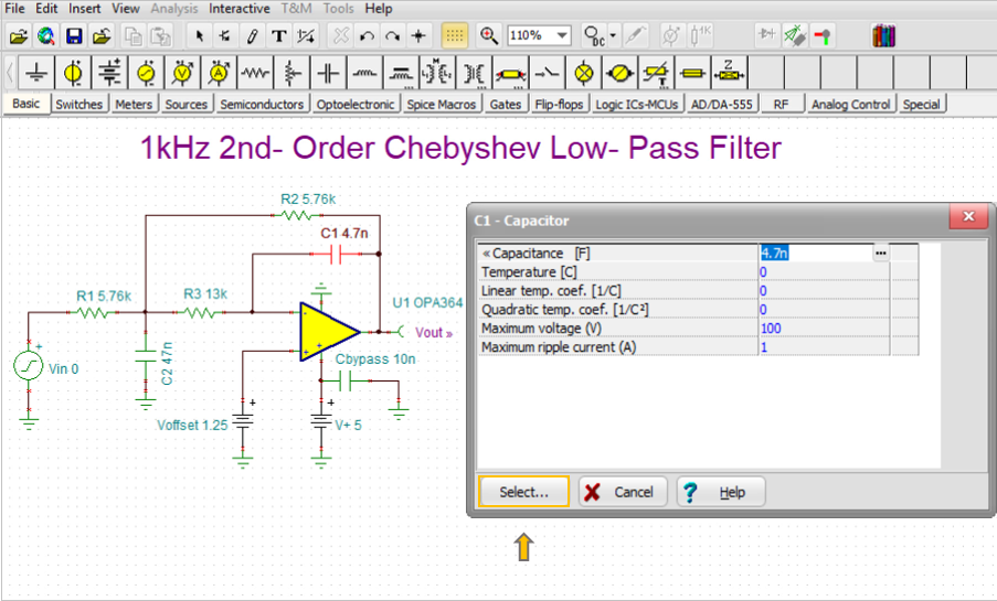
Press the select button. The following dialog will appear:
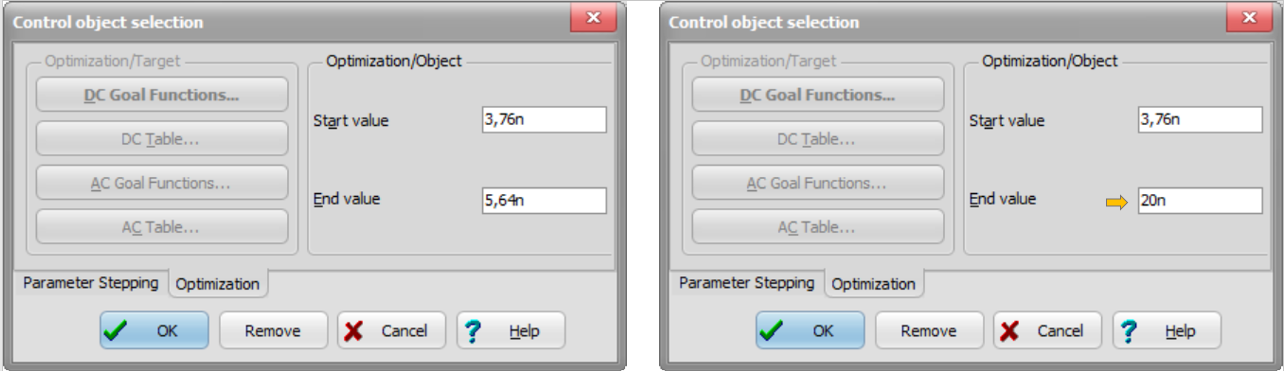
The program automatically sets a range (constraint) where the Optimum value will be searched. End value to 20n as shown above.
Now repeat the same procedure for R2. Set the End value to 20k.
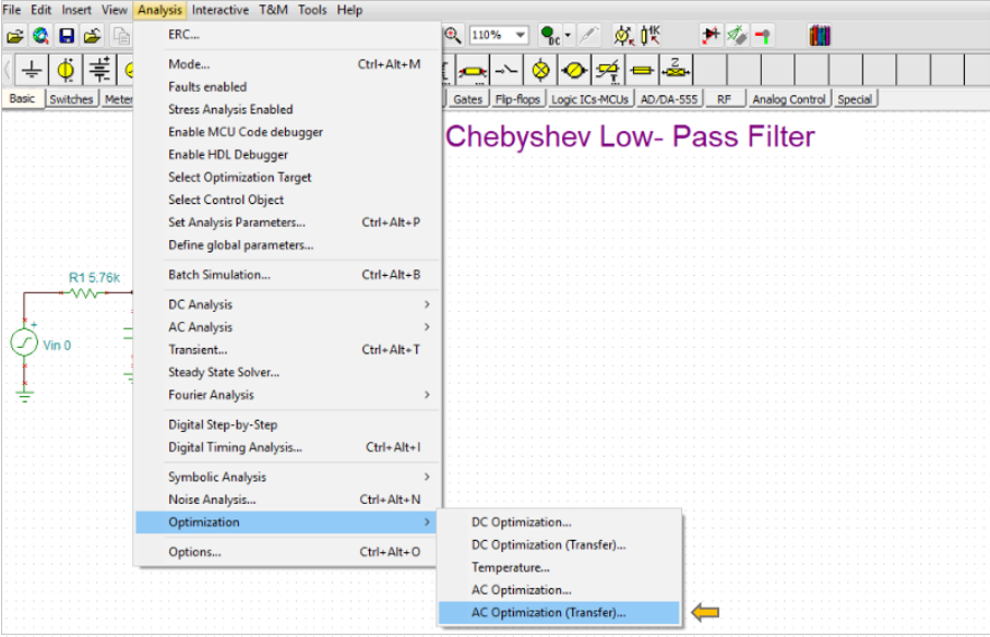
After finishing the Optimization setup, select Optimization/AC Optimization(Transfer) from the Analysis menu.
The following dialog will appear:
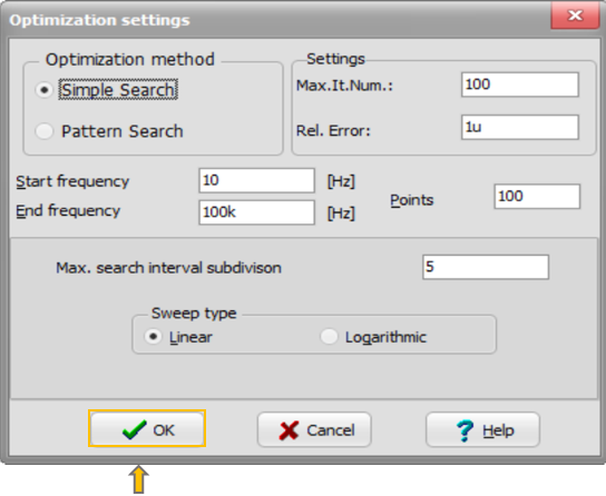
Accept the default settings by pressing OK.
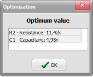
After a short calculation the optimum is found and changed component parameters appear:
Finally check the result with circuit simulation running Run AC Analysis/AC Transfer Characteristic.
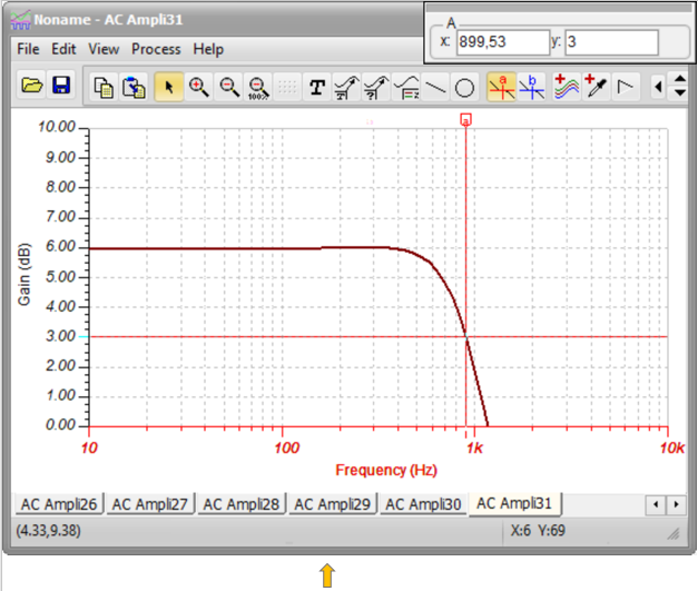
As shown on the diagram the target values (Gain 6db, Cut-off frequency 900Hz) have been reached.
Using the Circuit Designer Tool in TINA and TINACloud
Another method of method of designing circuits in TINA and TINAcloud is using the built is Circuit Designer tool called simply Design Tool.
Design Tool works with the design equations of your circuit to ensure that the specified inputs result in the specified output response. The tool requires of you a statement of inputs and outputs and the relationships among the component values. The tool offers you a solution engine that you can use to solve repetitively and accurately for various scenarios. The calculated component values are automatically set in place in the schematic and you can check the result by simulation.
Let’s design the AC amplification of the same circuit using our Circuit Designer tool.
Open the circuit from the Design Tool folder of TINACloud. The following screen will appear.
Now let’s run AC Analysis /AC Transfer Characteristic.
The following diagram will appear:
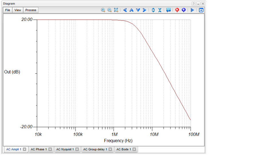
Now let’s redesign the circuit to have unity gain (0dB)
Invoke the Redesign this Circuit from the Tools menu
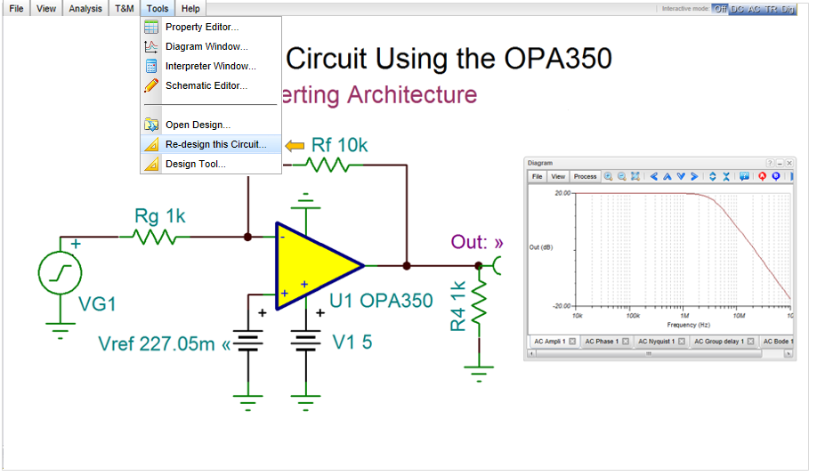
The following dialog will appear.
Set Gain to -1 (0 dB) and press the Run button.
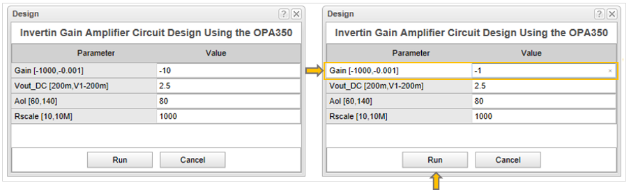
The calculated new component values will immediately appear in the schematic editor, drawn in red color.
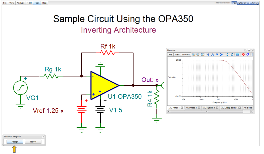
Press the Accept button.
The changes will be finalized. Run AC Analysis /AC Transfer Characteristics again to check the redesigned circuit.
———————————————————————————————————————————————————-
1This technique was devised by Phil Vrbancic, a student at California State University, Long Beach, and presented in a paper submitted to the IEEE Region VI Prize Paper Contest.