
3. The Typical Op-amp
 CURRENT – 3. The typical op-amp
 PREVIOUS- 2. Level shifters
The Typical Op-amp
Most operational amplifiers are designed and constructed in accordance with the block diagram shown in Figure 8.
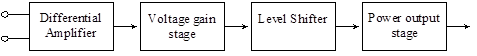
Figure 8 – Typical configuration of an op-amp
The differential amplifier and the voltage gain stage are the only stages which provide the voltage gain. The differential amplifier also provides the CMRR which is so important in the op-amp. The output of the differential amplifier is often connected to an emitter follower with a large emitter resistor so as to provide a high impedance load to the differential amplifier in order to obtain a high gain. Remember that a high-gain common-emitter amplifier suffers from much lower input impedance than a moderate gain CE amplifier. This then allows the use of a high gain CE amplifier to provide the additional gain. Linear op-amps are direct coupled to provide ac gain. This also eliminates the need for a coupling capacitor that is too large to be placed on an IC chip. Level shifters are required to insure that the output signal does not have any dc offset. Op-amps can be very accurately modeled by circuit simulation. We will demonstrate this using the TINACloud online circuit simulation.
3.1 Packaging
Op-amp circuits are packaged in standard IC packages, including cans, dual-in-line packages (DIP), and flat packs. Each of these packages has at least eight pins or connections. They are illustrated in Figures 9, 10, and 11.
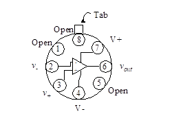
Figure 9 – Op-amp connection for can package (top view)
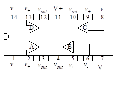
Figure 10 – Op-amp connection 14-pin DIP (Top View)
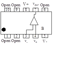
Figure 11 – Op-amp connection for 10-pin flat pack (Top view)
When constructing a circuit, it is important to identify the various leads correctly (they are usually not numbered). The figures illustrate the location of pin 1. In the can package of Figure 9, pin 1 is identified as the first pin to the left of the tab, and the pins are numbered consecutively counterclockwise looking from the top. In the dual-in-line package of Figure 10, the top of the package has an indentation to locate pin 1, and the pins are numbered down on the left and up on the right. Note that more than one op-amp (typically 2 or 4) is packaged in one DIP.
In the flat pack of Figure 11, pin 1 is identified by a dot and the pins are numbered as in the DIP.
3.2 Power Requirements
Many op-amps require both a negative and a positive voltage source. Typical voltage sources range from ±5 V to ±25 V. Figure 12 shows typical power supply connections to the op-amp.
The maximum output voltage swing is limited by the dc voltage supplied to the op-amp. Some operational amplifiers can be operated from a single voltage source. The manufacturer’s specifications define the limits of operation in those cases where the op-amp uses only one power supply.
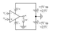
Figure 12 – Power supply connections
The maximum output voltage swing is limited by the dc voltage supplied to the op-amp. Some operational amplifiers can be operated from a single voltage source. The manufacturer’s specifications define the limits of operation in those cases where the op-amp uses only one power supply.
3.3 The 741 Op-amp
The μA741 op-amp is illustrated in the equivalent circuit of Figure 13. It has been produced since 1966 by most IC manufacturers, and although there have been many advances since its introduction, the 741 is still widely used.
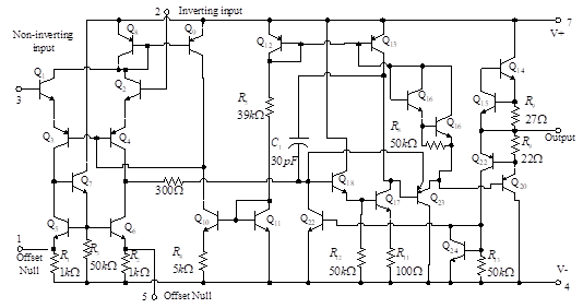
Figure 13 – The 741 op-amp
The 741 op-amp has internal compensation which refers to the RC network which causes the high-frequency amplitude response to fall off. Because the amplifier has high gain (on the order of 104 to 105 at low frequencies) and because parasitic capacitances in the transistors allow parasitic feedback, the op-amp would become unstable and oscillate if it were not for the internal compensation. Two cascaded difference amplifiers drive a complementary symmetry power amplifier through another voltage amplifier.
The 741 op-amp consists of three stages: an input differential amplifier, an intermediate single-ended high gain amplifier, and an output buffering amplifier. Other circuitry important to its operation is a level shifter to shift the dc level of the signal so that the output can swing both positive and negative, bias circuits to provide reference currents to the various amplifiers, and circuits that protect the op-amp from short circuits at the output. The 741 is internally compensated by means of an on-chip capacitor-resistor network.
The op-amp is further improved by adding more stages of amplification, isolating the input circuits, and adding more emitter followers at the output to decrease the output impedance. Other improvements result in increased CMRR, higher input impedance, wider frequency response, decreased output impedance and increased power.
Bias Circuits
Several constant sources can be seen in the 741 op-amp of Figure 13. Transistors Q8 and Q9 are the current source for IEE of the differential amplifier formed by Q1, Q2, Q3, and Q4. Transistors Q5, Q6, and Q7, are the active loads substituting for the RC resistors of the differential amplifier. Transistors Q10, Q11, and Q12 form the bias network for the differential amplifier current sources. Transistors Q10 and Q11 form a Widlar current source for this bias network with the other transistors acting as a current mirror.
Short Circuit Protection
The 741 circuit includes a number of transistors that are normally cut off and conduct only in the event that a large current exists at the output. The bias on the output transistors is then changed to reduce this current to an acceptable level. In the circuit of Figure 13, this short-circuit protection network consists of transistors Q15 and Q22 and resistor R11.
Input Stage
The input stage of the 741 op-amp is required to provide voltage gain, level shifting, and a single-ended differential amplifier output. The complexity of the circuitry causes a large offset voltage error. In contrast to this, the standard resistor-loaded differential amplifier causes less offset voltage error. However, the standard amplifier has limited gain which means that more stages would be required to achieve the desired amplification. The resistor-loaded differential amplifiers are used in op-amps which have less voltage drift than the 741.
BJTs used in the input stage require large bias currents, introducing offset current problems. To reduce the offset current error, other op-amp types use MOSFETs in the input stage.
The input stage of the 741 is a differential amplifier with an active load formed by transistors Q5, Q6, and Q7 and resistors R1, R2, and R3. This circuit provides a high resistance load and converts the signal from differential to single-ended with no degradation of gain or common-mode rejection ratio. The single-ended output is taken from the collector of Q6. The input stage level shifter consists of lateral pnp transistors, Q3 and Q4, which are connected in a common-base configuration.
Use of the lateral transistors, Q3 and Q4, results in an added advantage. They help protect the input transistors, Q1 and Q2, against emitter-base junction breakdown. The emitter-base junction of an npn transistor will break down when the reverse bias exceeds about 7 V. Lateral transistor breakdown does not occur until the reverse bias exceeds about 50 V. Since the transistors are in series with Q1 and Q2, the breakdown voltage of the input circuit is increased.
Intermediate Stage
The intermediate stages in most op-amps provide high gain through several amplifiers. In the 741, the single-ended output of the first stage is connected to the base of Q16 which is in an emitter follower configuration. This provides a high input impedance to the input stage which minimizes loading. The intermediate stage also consists of transistors Q16 and Q17, and resistors R8 and R9. The output of the intermediate stage is taken from the collector of Q17, and provided to Q14 through a phase splitter. The capacitor in the 741 is used for frequency compensation which is discussed in subsequent chapters of this text.
Output Stage
The output stage of an op-amp is required to provide high current gain to a low-output impedance. Most op-amps use a complementary symmetry output stage to increase efficiency without sacrificing current gain. The maximum achievable efficiency for the complementary symmetry, class B amplifier is 78% . The single-ended output amplifier has a maximum efficiency of only 25%. Some op-amps use Darlington pair complementary symmetry to increase their output capability. The complementary symmetry output stage in the 741 consists of Q14 and Q20.
The small resistors, R6 and R7, provide current limiting at the output. The Darlington pair, Q18 and Q19, is used in place of the diode in the diode-compensated complementary symmetry output stage as described in Chapter 8. The Darlington pair arrangement is favored over the two transistors connected as a diode since it can be fabricated in a smaller area. The current source substituting for the bias resistor in the complementary symmetry circuit is realized by one part of transistor Q13. Transistors Q22, Q23, and Q24 are part of a level shifter arrangement which insures that the output voltage is centered around the zero axis.
CURRENT – 3. The typical op amp