
5. Practical Op-amps
 CURRENT – 5. Practical Op-amps
 PREVIOUS- 4. Manufacturers’ specifications
Practical Op-amps
Practical Op-amps approximate their ideal counterparts but differ in some important respects. It is important for the circuit designer to understand the differences between actual op-amps and ideal op-amps, since these differences can adversely affect circuit performance.
Our goal is to develop a detailed model of the practical op-amp – a model that takes into account the most significant characteristics of the non-ideal device. We begin by defining the parameters used to describe practical op-amps. These parameters are specified in listings on data sheets supplied by the op-amp manufacturer.
Table 1 lists the parameter values for three particular op-amps, one of the three being the μA741. We use μA741 operational amplifiers in many of the examples and end-of-chapter problems for the following reasons: (1) they have been fabricated by many IC manufacturers, (2) they are found in great quantities throughout the electronics industry, and (3) they are general-purpose internally-compensated op-amps, and their properties can be used as a reference for comparison purposes when dealing with other op-amp types. As the various parameters are defined in the following sections, reference should be made to Table 9.1 in order to find typical values.
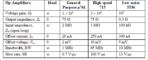
Table 1 – Parameter values for op-amps
The most significant difference between ideal and actual op-amps is in the voltage gain. The ideal op-amp has a voltage gain that approaches infinity. The actual op-amp has a finite voltage gain that decreases as the frequency increases (we explore this in detail in the next chapter).
5.1 Open-Loop Voltage Gain (G)
The open-loop voltage gain of an op-amp is the ratio of the change in output voltage to a change in the input voltage without feedback. Voltage gain is a dimensionless quantity. The symbol G is used to indicate the open-loop voltage gain. Op-amps have high voltage gain for low-frequency inputs. The op-amp specification lists the voltage gain in volts per millivolt or in decibels (dB) [defined as 20log10(vout/vin)].
5.2 Modified Op-amp Model
Figure 14 shows a modified version of the idealized op-amp model. We have altered the idealized model by adding input resistance (Ri), output resistance (Ro), and common-mode resistance (Rcm).
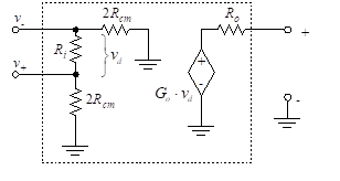
Figure 14 – Modified op-amp model
Typical values of these parameters (for the 741 op-amp) are
We now consider the circuit of Figure 15 in order to examine op-amp performance. The inverting and non-inverting inputs of the op-amp are driven by sources that have series resistance. The output of the op-amp is fed back to the input through a resistor, RF.
The sources driving the two inputs are denoted vA and v1, and the associated series resistances are RA and R1. If the input circuitry is more complex, these resistances can be considered as Thevenin equivalents of that circuitry.
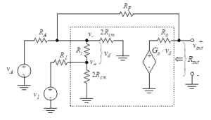
Figure 15 – Op-amp circuit
5.3 Input Offset Voltage (Vio)
When the input voltage to an ideal op-amp is zero, the output voltage is also zero. This is not true for an actual op-amp. The input offset voltage, Vio, is defined as the differential input voltage required to make the output voltage equal to zero. Vio is zero for the ideal op-amp. A typical value of Vio for the 741 op-amp is 2 mV. A non-zero value of Vio is undesirable because the op-amp amplifies any input offset, thus causing a larger output dc error.
The following technique can be used to measure the input offset voltage. Rather than vary the input voltage in order to force the output to zero, the input is set equal to zero, as shown in Figure 16, and the output voltage is measured.
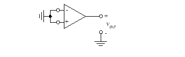
Figure 16 – Technique for measuring Vio
The output voltage resulting from a zero input voltage is known as the output dc offset voltage. The input offset voltage is obtained by dividing this quantity by the open-loop gain of the op-amp.
The effects of input offset voltage can be incorporated into the op-amp model as shown in Figure 17.
In addition to including input offset voltage, the ideal op-amp model has been further modified with the addition of four resistances. Ro is the output resistance. The input resistance of the op-amp, Ri, is measured between the inverting and non-inverting terminals. The model also contains a resistor connecting each of the two inputs to ground.
These are the common-mode resistances, and each is equal to 2Rcm. If the inputs are connected together as in Figure 16, these two resistors are in parallel, and the combined Thevenin resistance to ground is Rcm. If the op-amp is ideal, Ri and Rcm approach infinity (i.e., open circuit) and Ro is zero (i.e., short circuit).
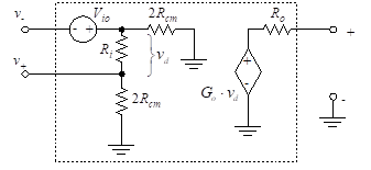
Figure 17 – Input offset voltage
The external configuration shown in Figure 18(a) can be used to negate the effects of offset voltage. A variable voltage is applied to the inverting input terminal. Proper choice of this voltage cancels the input offset. Similarly, Figure 18(b) illustrates this balancing circuit applied to the non-inverting input.
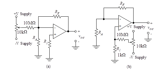
Figure 18 – Offset voltage balancing
APPLICATION
You can test the Input Offset Voltage Balancing of the 18 (a) circuit by simulation online with the TINACloud Circuit Simulator by clicking the link below.
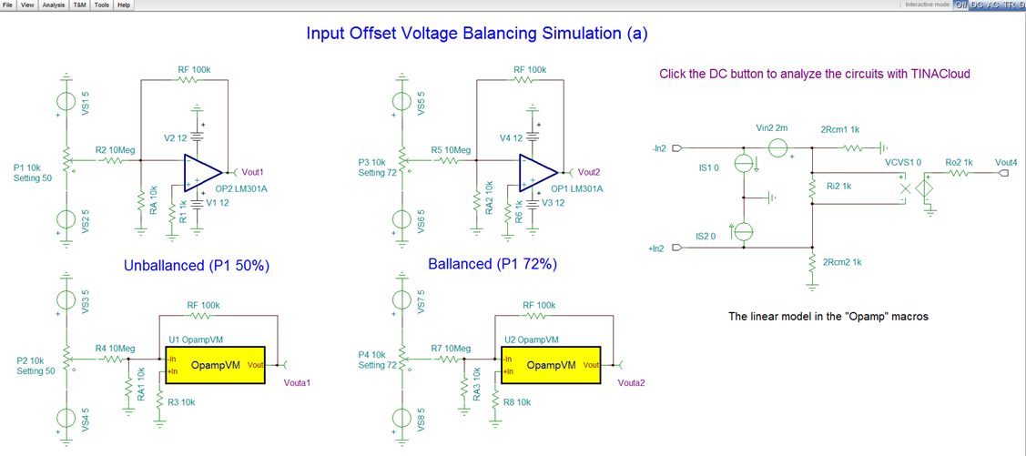
Input Offset Voltage Balancing Circuit Simulation (a) with TINACloud
Input Offset Voltage Balancing Circuit Simulation (a) with TINACloud
APPLICATION
You can test the Input Offset Balancing of the 18 (b) circuit by simulation online with the TINACloud Circuit Simulator by clicking the link below:
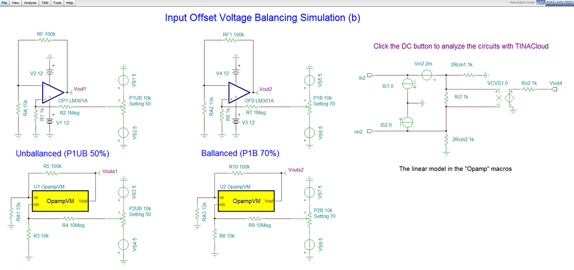
Input Offset Voltage Balancing Circuit Simulation (b) with TINACloud
Input Offset Balancing Circuit Simulation (b) with TINACloud
5.4 Input Bias Current (IBias)
Although ideal op-amp inputs draw no current, actual op-amps allow some bias current to enter each input terminal. IBias is the dc current into the input transistor, and a typical value is 2 μA. When the source impedance is low, IBias has little effect, since it causes a relatively small change in input voltage. However, with high-impedance driving circuits, a small current can lead to a large voltage.
The bias current can be modeled as two current sinks, as shown in Figure 19.
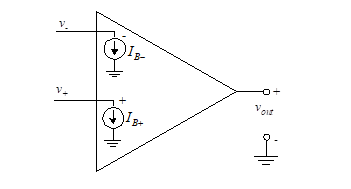
Figure 19 – Offset voltage balancing
The values of these sinks are independent of the source impedance. The bias current is defined as the average value of the two current sinks. Thus
(40)
The difference between the two sink values is known as the input offset current, Iio, and is given by
(41)
Both the input-bias current and the input offset current are temperature dependent. The input bias current temperature coefficient is defined as the ratio of change in bias current to change in temperature. A typical value is 10 nA/oC. The input offset current temperature coefficient is defined as the ratio of the change in magnitude of the offset current to the change in temperature. A typical value is -2nA/oC.
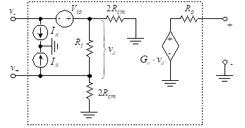
Figure 20 – Input bias current model
The input bias currents are incorporated into the op-amp model of Figure 20, where we assume that the input offset current is negligible.
That is,![]()
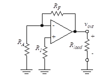
Figure 21(a) – The circuit
We analyze this model in order to find the output voltage caused by the input bias currents.
Figure 21(a) shows an op-amp circuit where the inverting and non-inverting inputs are connected to ground through resistances.
The circuit is replaced by its equivalent in Figure 21(b), where we have neglected Vio. We further simplify the circuit in Figure 21(c) by neglecting Ro and Rload. That is, we assume RF >> Ro and Rload >> Ro. Output loading requirements usually ensure that these inequalities are met.
The circuit is further simplified in Figure 21(d) where the series combination of the dependent voltage source and resistor is replaced by a parallel combination of a dependent current source and resistor.
Finally, we combine resistances and change both current sources back to voltage sources to obtain the simplified equivalent of Figure 21(e).
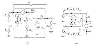
Figure 21(b) and (c) – Input bias effects
We use a loop equation to find the output voltage.
(43)
where
(44)
The common-mode resistance, Rcm, is in the range of several hundred megohms for most op-amps. Therefore
(45)
If we further assume that Go is large, Equation (43) becomes Equation .
(46)
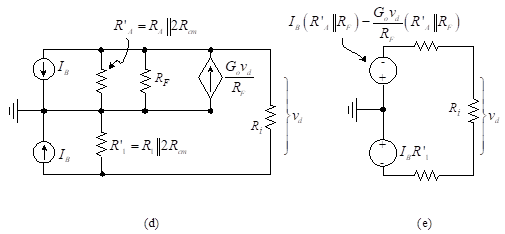
Figure 21(d) and (e) – Input bias effects
Note that if the value of R1 is selected to be equal to , then the output voltage is zero. We conclude from this analysis that the dc resistance from V+ to ground should equal the dc resistance from V– to ground. We use this bias balance constraint many times in our designs. It is important that both the inverting and non-inverting terminals have a dc path to ground to reduce the effects of input bias current.
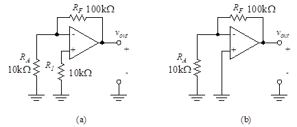
Figure 22 – Configurations for Example 1
Example 1
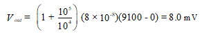
Find the output voltage for the configurations of Figure 22 where IB = 80 nA = 8 10-8 A.
Solution: We use the simplified form of Equation (46) to find the output voltages for the circuit of Figure 22(a).
![]()
For the circuit of Figure 22(b), we obtain
APPLICATION
Also, you can carry out these calculations with TINACloud circuit simulator, using its Interpreter tool by clicking the link below.
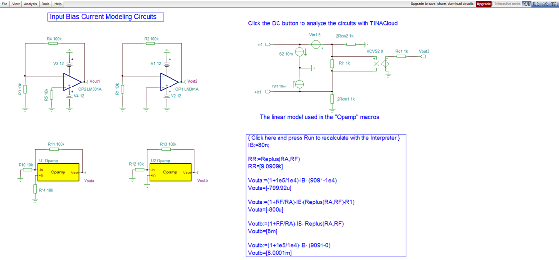
Input Bias Current Modeling Circuit Simulation with TINACloud
Input Bias Current Modeling Circuit Simulation with TINACloud
5.5 Common-Mode Rejection
The op-amp is normally used to amplify the difference between two input voltages. It therefore operates in the differential mode. A constant voltage added to each of these two inputs should not affect the difference and should therefore not be transferred to the output. In the practical case, this constant, or average value of the inputs does affect the output voltage. If we consider only the equal parts of the two inputs, we are considering what is known as the common mode.
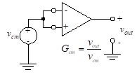
Figure 23 – Common mode
Let us assume that the two input terminals of an actual op-amp are connected together and then to a common source voltage. This is illustrated in Figure 23. The output voltage would be zero in the ideal case. In the practical case, this output is non-zero. The ratio of the non-zero output voltage to the applied input voltage is the common-mode voltage gain, Gcm. The common-mode rejection ratio (CMRR) is defined as the ratio of the dc open-loop gain, Go, to the common mode gain. Thus,
(47)
Typical values of the CMRR range from 80 to 100 dB. It is desirable to have the CMRR as high as possible.
5.6 Power Supply Rejection Ratio
Power supply rejection ratio is a measure of the ability of the op-amp to ignore changes in the power supply voltage. If the output stage of a system draws a variable amount of current, the supply voltage could vary. This load-induced change in supply voltage could then cause changes in the operation of other amplifiers sharing the same supply. This is known as cross-talk, and it can lead to instability.
The power supply rejection ratio (PSRR) is the ratio of the change in vout to the total change in power supply voltage. For example, if the positive and negative supplies vary from ±5 V to ±5.5 V, the total change is 11 – 10 = 1 V. The PSRR is usually specified in microvolts per volt or sometimes in decibels. Typical op-amps have a PSRR of about 30 μV/V.
To decrease changes in supply voltage, the power supply for each group of op-amps should be decoupled (i.e., isolated) from those of other groups. This confines the interaction to a single group of op-amps. In practice, each printed circuit card should have the supply lines bypassed to ground via a 0.1-μF ceramic or 1-μF tantalum capacitor. This ensures that load variations will not feed significantly through the supply to other cards.
5.7 Output Resistance
As a first step in determining the output resistance, Rout, we find the Thevenin equivalent for the portion of the op-amp circuit shown in the box enclosed in dashed lines in Figure 24. Note that we are ignoring the offset current and voltage in this analysis.
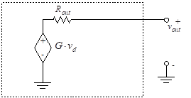
(24)
Since the circuit contains no independent sources, the Thevenin equivalent voltage is zero, so the circuit is equivalent to a single resistor. The value of the resistor cannot be found using resistor combinations. To find the equivalent resistance, assume that a voltage source, v, is applied to the output leads. We then calculate the resulting current, i, and take the ratio v/i. This yields the Thevenin resistance.
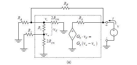
Figure 25 (part a) – Thevenin equivalent circuits
Figure 25 (part b)
Figure 25(a) illustrates the applied voltage source. The circuit is simplified to that shown in Figure 25(b).
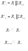
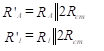
The circuit can be further reduced to that shown in Figure 25(c), where we define two new resistances as follows:
(48)
We make the assumption that R’A << (R’1 + Ri) and Ri >> R’1. The simplified circuit of Figure 25(d) results.
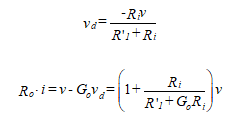
The input differential voltage, vd, is found from this simplified circuit using a voltage divider ratio.
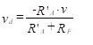
(49)
To find the output resistance, we begin by writing the output loop equation.
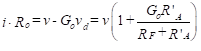
(50)
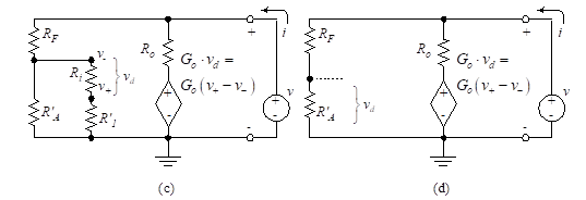
Figure 25 (parts c and d) – Reduced Thevenin equivalent circuits
The output resistance is then given by Equation (51).
(51)
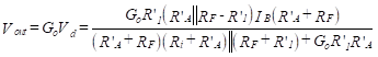
In most cases, Rcm is so large that R’A»RA and R1‘»R1. Equation (51) can be simplified using the zero-frequency voltage gain, Go. The result is Equation (52).
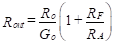
(52)
APPLICATION
You can calculate the Output Impedance of the circuit 25 (a) with circuit simulation using the TINACloud Circuit Simulator by clicking the link below.
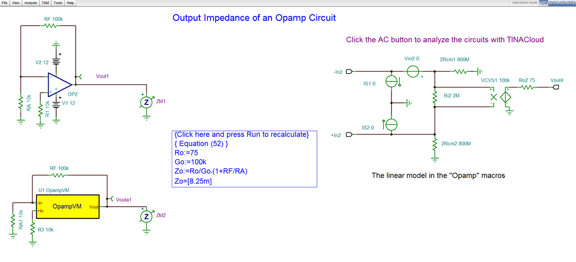
Output Impedance of an Opamp Circuit Simulation with TINACloud
Output Impedance of an Opamp Circuit Simulation with TINACloud
Example 2
Find the output impedance of a unity-gain buffer as shown in Figure 26.
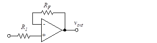
Figure 26 – Unity gain buffer
Solution: When the circuit of Figure 26 is compared to the feedback circuit of Figure 24, we find that
![]()
Therefore,
![]()
Equation (51) cannot be used, since we are not sure that the inequalities leading to the simplification of Figure 25(c) apply in this case. That is, the simplification requires that
![]()
Without this simplification, the circuit takes the form shown in Figure 27.
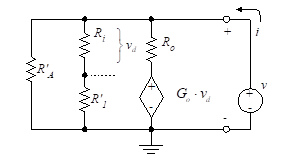
Figure 27 – Equivalent circuit for Unity gain buffer
This circuit is analyzed to find the following relations:
In the first of these equations, we have assumed that Ro<<(R’1+Ri)<<2Rcm. The output resistance is then given by
![]()
Where we again use the zero-frequency voltage gain, Go.