
8. Inverting Amplifier
 CURRENT – 8. Inverting Amplifier
 PREVIOUS- 7. Non-inverting amplifier
Figure 36(a) illustrates an inverting amplifier. Figure 36(b) shows the equivalent circuit using the op-amp model developed earlier in this chapter.
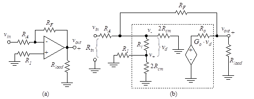
Figure 36 – Inverting amplifier
8.1 Input and Output Resistance
Figure 36(b) is reduced to Figure 37(a) if we let, ![]()
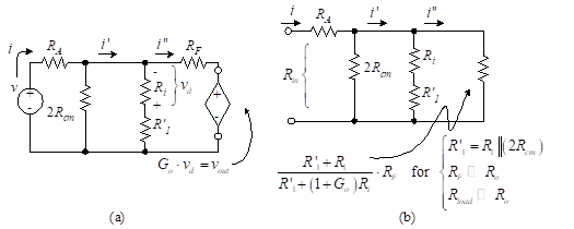
Figure 37 – Simplified inverting amplifier model
It is reasonable to assume that these inequalities apply because, were they not true, the output would load the input and the gain would be reduced.
A voltage-divider relationship can be used to yield
(71)
and a loop equation yields
(72)
The input resistance, Rin, is obtained from Figure 37(b), where we have replaced the dependent source with an equivalent resistance. The value of this resistor is v–/i” which is found from Equation (72) . For large G (i.e., ![]() ), the rightmost resistance in Figure 37(b) is approximately zero, and
), the rightmost resistance in Figure 37(b) is approximately zero, and ![]() .
.
The output resistance of the inverting amplifier is the same as that of the non-inverting amplifier. Thus,
(73)
8.2 Voltage Gain
We use the equivalent circuits of Figure 36(b) and Figure 37(a) to determine the voltage gain. The inverting input gain, A– = vout/vin, is obtained from the circuit of Figure 37(a) by again making the same assumptions that we made in finding the output resistance.
These assumptions reduce the circuit to that shown in Figure 38(a), where we have changed the voltage source in series with a resistance to a current source in parallel with a resistance. The resistors can then be combined to yield the circuit of Figure 38(b). Finally, the current source is converted back to the voltage source to yield the simplified circuit of Figure 38(c).
The loop equation for this circuit is given by
(74)
Since vout = Govd, the inverting voltage gain is
(75)
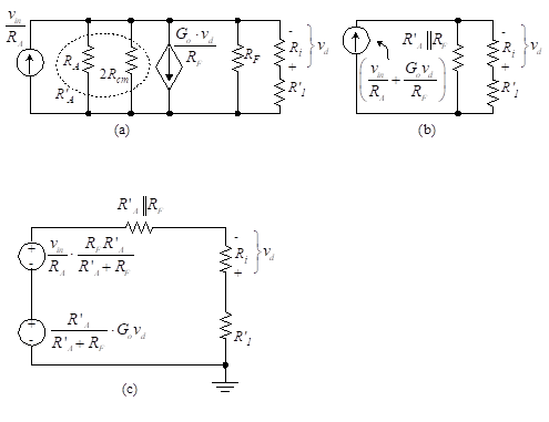
Figure 38 (parts a, b, c)- Inverting input gain
We can verify this result relative to the gain of the ideal op-amp by making the approximations: RA << 2Rcm and G >> 1. Then
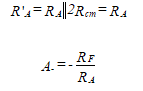
(76)
This is the same as the result found earlier for the simplified model.
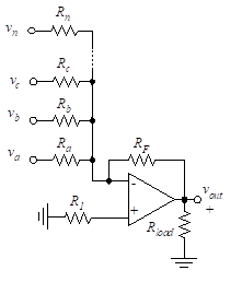
8.3 Multiple-Input Amplifiers
(39)
If the voltages va, vb, … , vm are applied to the summing junction (inverting input to op-amp) through resistors Ra, Rb, …, Rm, respectively, as shown in Figure 39, the output voltage is
(77)
To achieve bias balance, we choose
(78)
Let us define
![]()
(79)
The output resistance is then
(80)
Suppose now that only two inputs are used. The output voltage is then
(81)
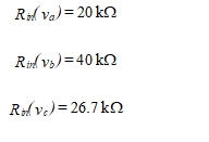
The input resistance at va is approximately equal to Ra, and the input resistance at vb is approximately Rb. We can make this circuit a unity-gain two-input summer with an output voltage of
(82)
by setting RF = Ra = Rb. The resistance from the non-inverting input terminal to ground is chosen to achieve bias balance. Thus, R1 = RF/3, and we have
(83)
An equal-gain (i.e., not unity) two-input summer is obtained by setting ![]() and
and ![]() . In this case, the output voltage is
. In this case, the output voltage is
(84)
The input resistance is approximately R. Since RA = R/2,
(85)
If m inputs are summed through equal resistors (say R), the output voltage is
(86)
For this equal-gain multiple-input inverting summer, the input resistance to each input is approximately R. Since RA = R/m,
(87)
and
(88)
The output resistance is
(89)
Example
Design and analyze a three-input inverting amplifier using a 741 op-amp where
![]()
and the input resistance is Rmin = 8 kΩ.
Solution: We use the design method of Chapter “Ideal Operational Amplifiers” to find X = 0, Y = 9, Z = -10.
Then
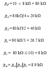
The gain multiplier of the amplifier is 1+RF/RA = 10. We find the input resistance as follows:
The output resistance is approximately 75(10)/105 = 7.5 mΩ. To achieve bias balance, we set
![]()