
7. Non-inverting Amplifier
 CURRENT – 7. Non-inverting Amplifier
 PREVIOUS- 6. Computer Simulation of Op-amp circuits
Non-inverting Amplifier
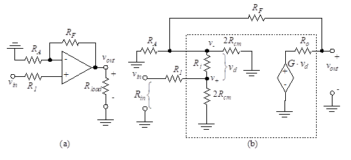
Figure 29 – The non-inverting amplifier
Figure 29(a) illustrates the non-inverting amplifier, and Figure 29(b) shows the equivalent circuit.
The input voltage is applied through R1 into the non-inverting terminal.
7.1 Input and Output Resistances
The input resistance of this amplifier is found by determining the Thevenin equivalent of the input circuit. The load resistance is normally such that Rload >> Ro. If this were not true, the effective gain would be reduced and the effective value of Ro would be the parallel combination of Ro with Rload. Let us again define and R’F = RF + Ro. We shall neglect R1, since it is so much less than Rin. Now since Rload >> Ro, we can reduce Figure 29(a) to the simplified form of Figure 30(a).
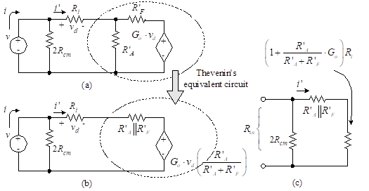
Figure 30 – Reduced circuits for input resistance
We find the Thevenin equivalent of the circuit surrounded by the elliptical curve, resulting in Figure 30(b). In Figure 30(c), the resistance to the right of 2Rcm is given by v/i’. In order to evaluate this, we write a loop equation to obtain
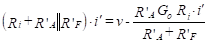
(53)
Therefore,
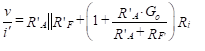
(54)
The input resistance is the parallel combination of this quantity with 2Rcm.
(55)
Recall that , R’F = RF + Ro, and Rload >> Ro. If we retain only the most significant terms and note that Rcm is large, Equation (55) reduces to
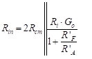
(56)
where we again use the zero-frequency voltage gain, Go.
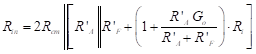
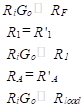
Equation (56) can be used to find the input resistance of the 741 op-amp. If we substitute the parameter values as given in Table 1, Equation (56) becomes
![]()
We again use the assumptions that Rcm is large, that is R’F » RF and R’A » RA. Then the output resistance of a 741 op-amp is given by
(57)
EXAMPLE
Calculate the input resistance for the unity-gain follower shown in Figure 31(a).
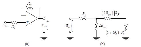
Figure 31 – Unity-gain follower
Solution: The equivalent circuit is shown in Figure 31(b). Since we assume the zero-frequency gain, Go, and the common-mode resistance, Rcm, are high, we can neglect the term ![]() compared to (1+Go)Ri. Equation (57) cannot be used since RA = 0. The input resistance is then given by
compared to (1+Go)Ri. Equation (57) cannot be used since RA = 0. The input resistance is then given by
![]()
This is typically equal to 400 MΩ or more, so we can neglect R1 (i.e., set R1 = 0).
7.2 Voltage Gain
We wish to determine the voltage gain, A+ for the non-inverting amplifier of Figure 32(a).
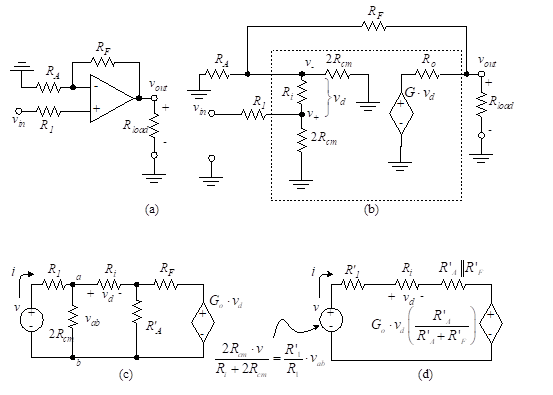
Figure 32 – Non-inverting amplifier
This gain is defined by
(58)
The equivalent circuit is shown in Figure 32(b). If we assume RF>>Ro, Rload>>Ro and , the circuit can be reduced to that shown in Figure 32(c). If we further define , then Figure 32(d) results.
The assumed conditions are desirable in order to prevent reduction of the effective gain. The operation of taking Thevenin equivalents modifies the dependent voltage source and the driving voltage source as in Figure 32(d). Note that
(59)
The output voltage is given by
(60)
We can find i by applying KVL to the circuit of Figure 32(d) to obtain
(61)
(62)
where
and ![]() implying
implying ![]() .
.
Solving for the current, i, we obtain
(63)
The voltage gain is given by the ratio of output to input voltage.
(64)
As a check of this result, we can reduce the model to that of the ideal op-amp. We use the zero-frequency gain, Go, in place of G in Equation (64) and also the following equalities.
(65)
When we let ![]() , Equation (64) becomes
, Equation (64) becomes
(66)
which agrees with the result for the idealized model.
Example
Find the gain of the unity-gain follower shown in Figure 33.
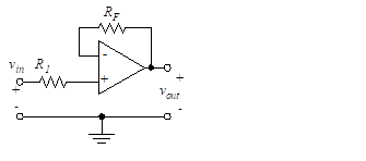
Figure 33 – Unity gain followerSolution: In this circuit, ![]() , R’A = 2Rcm, and RF << R’A. We assume that Go is large,
, R’A = 2Rcm, and RF << R’A. We assume that Go is large, ![]() , and we set R1 = RF. Equation (64) then reduces to
, and we set R1 = RF. Equation (64) then reduces to
![]()
(67)
so vout = vin as expected.
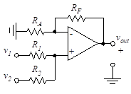
7.3 Multiple-Input Amplifiers
We extend the previous results to the case of the non-inverting amplifier with multiple voltage inputs. Figure 34 shows a multiple-input non-inverting amplifier.
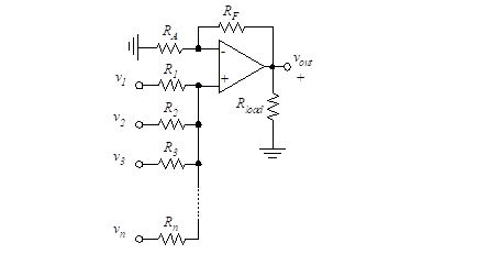
Figure 34 – Multiple-input non-inverting amplifier
If inputs v1, v2, v3, …, vn are applied through input resistances R1, R2, R3, …, Rn, we obtain a special case of the general result derived in Chapter “Ideal Operational Amplifiers”, as follows:
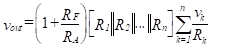
(68)
We choose
(69)
to achieve bias balance. The output resistance is found from Equation (52).
As a specific example, let us determine the output voltage of the two-input summer of Figure 35.
(35)
The output voltage is found from Equation (68) , as follows:
(70)
We choose ![]() to achieve bias balance. If we assume RF = R1 = R2 = RA, then Equation (70) reduces to vout = v1 + v2, which is a unity-gain two-input summer.
to achieve bias balance. If we assume RF = R1 = R2 = RA, then Equation (70) reduces to vout = v1 + v2, which is a unity-gain two-input summer.