9. Differential Summing
 CURRENT – 9. Differential Summing
 PREVIOUS- 8. Inverting Amplifier
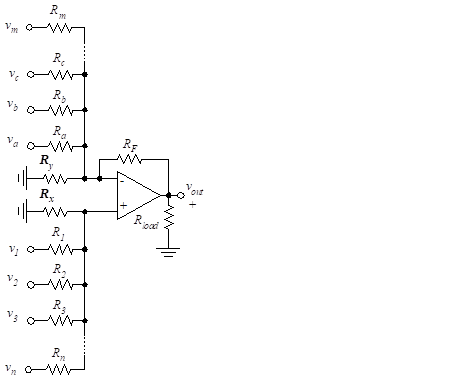
Figure 40 – Differential summing
We have seen that an op-amp can be configured to produce an output that is a weighted sum of multiple inputs. If the sum includes both positive and negative signs, Differential Summing results.
The op-amp configuration of Figure 40 produces an output voltage, vout, given by
(90)
where
(91)
We choose the resistors to achieve bias balance, as follows:
(92)
The input resistance for each inverting input, vj, is Rj.
If the inverting and non-inverting terminals each have only one input, the result is a differencing amplifier. This is illustrated in Figure 41.
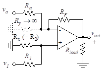
Figure 41 – Differencing amplifier
The output voltage for this configuration is
(93)
Note that RA = Ra [see Equation 91]. To achieve bias balance, we choose
(94)
The input resistance for the va terminal is RA. The input resistance for the v1 terminal is ![]() , where Rin is found from Equation (56) to be
, where Rin is found from Equation (56) to be
(95)
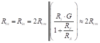
Then Rin(at V1) is approximately R1+R2. Rout is found in Equation (52) and is equal to
(96)
To achieve unit-gain differencing, where the output is given by vout = v1 – va we set RA = RF = R1 = Rx. If a 741 op-amp is used, a typical value for these four resistors is 10 kΩ.
The input resistance into vout is then 10 kΩ and into the v1 terminal the resistance is 20 kΩ.
Suppose that equal-gain differencing is desired but that the gains need not be unity. We then set R1 = RA and Rx = RF. The output voltage is then
(97)
The input resistance into the va terminal is ![]() , and into the non-inverting terminal it is , which is approximately RA + RF since Rin >> RF. Values for input resistance and Rout are easily determined with the use of Equations (95) and (96).
, and into the non-inverting terminal it is , which is approximately RA + RF since Rin >> RF. Values for input resistance and Rout are easily determined with the use of Equations (95) and (96).
A useful modification of the differencing amplifier configuration of Figure 41 is the sign switcher as shown in Figure 42.
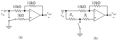
Figure 42 – Sign switcher
With the switch in the position shown in Figure 42(a), vout = –vin, and for the opposite switch position, vout = 2vin – vin = vin. The input resistance is 10 kΩ for each position, and the bias is balanced in each position. Figure 42(a) shows a single-pole double-throw switch. Sign switching can also be accomplished with a single-throw switch as shown in Figure 42(b). However, for this implementation, the bias and input resistances are not equal in the two switch positions.
Example
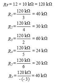
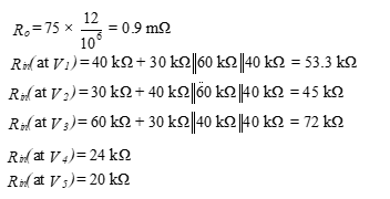
Determine the output resistance and the input resistance at each of the inputs of a multiple input 741 amplifier which has an output of
![]()
Assume that the value of the resistance at the + and – terminals is 10 kΩ.
Solution: Using the larger of X and (Y+1) yields the multiplying factor for determining RF.
![]() , then
, then
![]()
The circuit is shown in Figure 43.
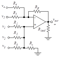
Figure 43-Circuit for Example