Circuit Design Tool in TINA
Circuit Design Tool in TINA
Jump to TINA Main Page & General Information
TINA is not only a circuit simulator but also a very powerful circuit designer.
The simplest way of circuit design with TINA is to check the circuit responses by simulation and modify circuit parameters so that the network produces the target output values. Beyond that, TINA also provides several tools for direct circuit design.
TINA’s Circuit Design Tool works with the design equations of your circuit to ensure that the specified inputs result in the specified output response. The tool requires of you a statement of inputs and outputs and the relationships among the component values. The tool offers you a solution engine that you can use to solve repetitively and accurately for various scenarios. The calculated component values are automatically set in place in the TINA schematic and you can check the result by simulation.
As an example, this tool can calculate feedback or other resistor and capacitor values of an amplifier in order to achieve a certain gain and bandwidth, and it can calculate component parameters of power supply circuits to meet output voltage and ripple requirements.
TINA’s Designer Tool promotes good documentation by storing the design procedure together with the circuit.
It is also very useful for semiconductor and other electronics component manufacturers to provide application circuits along with the design procedure.
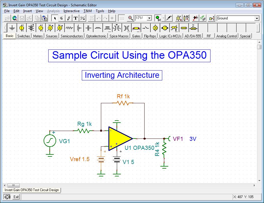
Let’s demonstrate the use of this tool through a simple operational amplifier example.
Open the Invert Gain OPA350 Test Circuit Design.TSC circuit from the ExamplesDesign Tool folder of TINA.
In the TINA Schematic Editor the following circuit will appear:
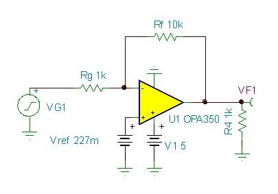
With the Design Tool we will set Rf and Vref to achieve the specified Gain and DC output voltage.
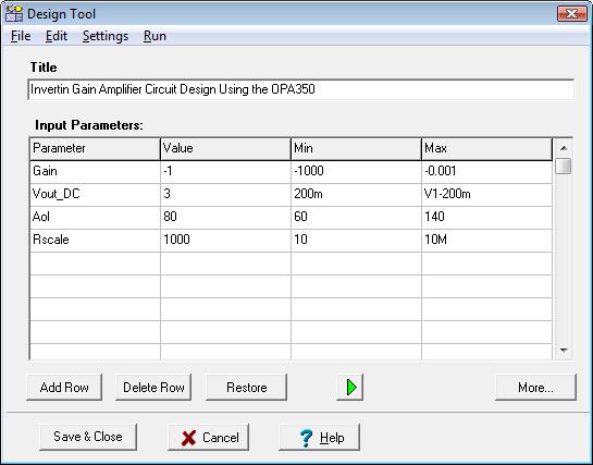
Now invoke the Design Tool from the Tools menu of TINA.
The following dialog will appear:
Note that in the Design Tool dialog you can also refer to component parameter names.
For example in the Vout_DC line the maximum value is set as V1-200m, telling that the DC output voltage must be at least by 200mV less than the V1 supply voltage of the IC.
If you just want to Run the design procedure press the Green Run button or the F9 key or use the Run command in the menu of the tool.
If you run TINA in interactive mode you can immediately see the effect of the changes made by the Design Tool.
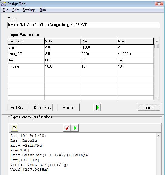
To see the design procedure itself, press the More button in the dialog.
The code of the design procedure, written in TINA’s Interpreter, will appear:
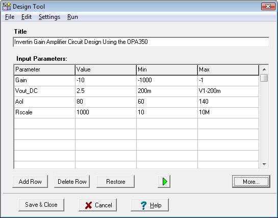
Now let’s change the Gain input parameter to -1, Vout_DC to 3V and run the procedure by clicking Run in the menu or pressing the green button or F9 on the keyboard.
In the code part we will see:
A:= 10^(Aol/20)
Rg:= Rscale
Rf:=-Gain*Rg*(1 + 1/A)/(1+Gain/A)
Rf=[1.0002k]
Vref:= Vout_DC/(1+Rf/Rg)
Vref=[1.4998]
The new values will immediately appear in the schematic editor, drawn in brown color.
Press the green DC button to display the DC output voltage:
Now run an AC Transfer analysis, the Bode diagram will appear:
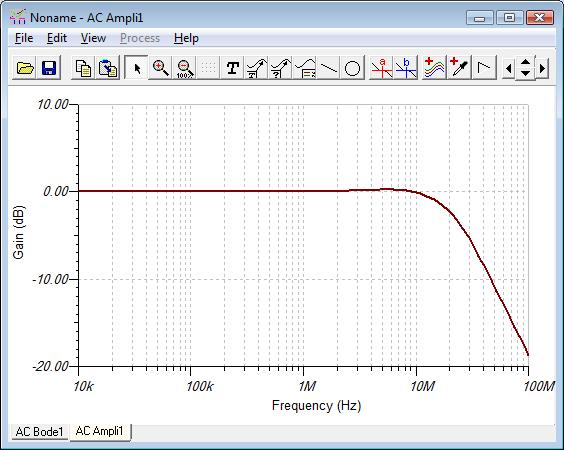
The small frequency Gain is 0dB which complies with the specified Vout/Vin=-1 value.
You can find more complex examples in the Design Tool folder of TINA.
You can make your own circuit design procedure in any TINA circuits and save it together with the circuit itself.