IBIS Simulation
IBIS Simulation
Jump to TINA Main Page & General Information
IBIS Simulation
IBIS (Input/Output Buffer Information Specification) is a method to provide modeling information about the input/output buffers of integrated circuits. The good thing about IBIS models is that they are often available even for devices where complete device models are not available from manufacturers for any reason (e.g., complexity, proprietary information protection, etc.).
One of the most popular uses of IBIS models is Signal Integrity Analysis, including impedance matching and more.
TINA currently supports the most widely used IBIS 4.2 version.
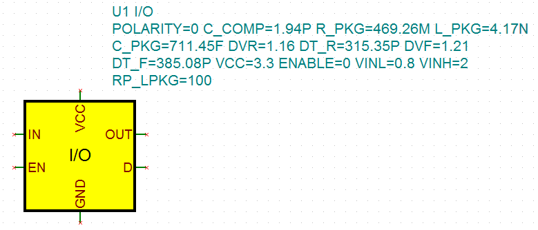
In TINA, you can convert IBIS models to TINA Spice macros and then use them in any circuits in TINA. You can also complete simplified digital device models—e.g., MCUs with IBIS models—to better describe their analog behavior.
In the following, we will show the use of IBIS models through an example of fixing signal integrity between a Texas Instrument TMS320C6748 DSP and an ADS1259 delta-sigma ADC.
Select File/Import/IBIS File (*.ibs), select c6748zce.ibs from < TINA directory >\Examples\IBIS.
The following dialog will be displayed. In this dialog, you can select the model to import.

Now select SPI1CLK_GP213 signal, PBFZP18LL_X50_PI_3P3 model (cell operated at 3.3V without pullup or pulldown), and Typ value set.
Press OK. The IBIS model is automatically converted to a Spice macro.
SPI1CLK_GP213 is the master configuration serial clock signal of TMS320C6748 chip to drive SPI clock input of an AD converter, Texas Instruments ADS1259.
Select File/Import/IBIS File (*.ibs), select ads1259.ibs from < TINA directory >\Examples\IBIS.
The following dialog will be displayed. In this dialog, you can select the model to import.

Now select SCK input signal, DIN_PD_3 model and Max value (for 3.3V DVDD voltage range).
Press OK. The IBIS model is automatically converted to a Spice macro.

Connect the DSP I/O buffer to the input of the ADC with a lossless transmission line.
Add the power source and voltage generator to create clock signal of DSP side. Place voltage pins for the simulation onto the signal nodes.
We adjust the transmission line parameters to a few inches of microstrip trace routed on a four-layer PCB. This produces cc. 500ps delay and 90 Ohms characteristic impedance.
File from <TINA directory>\Examples\IBIS\ Impedance matching of TMS320C6748.TSC is ready to be used.

Now, click Analysis, Transient.
The DSP transmits the SPI clock signal where the impedance mismatch creates reflections. The result shows the reflections created by the impedance mismatches in this circuit simulation.
At the ADC side (pin EoTL), the voltage is beyond the ground and the supply voltage, which violates the absolute maximum rating of the digital input.

To avoid under and overshoots at the line end is to match the output impedance of the driver to the trace impedance by inserting a resistor between the output and the trace.
Let us place a 100 Ω resistor in series now with the output.

Run the Transient Analysis again, and compare the results by copying the important curves with each other.

Now, we can see that using the IBIS model to understand and find the critical issues with the simulation helped to solve this problem.